ZHCSJE4B September 2017 – February 2019 TPS61085A-Q1
PRODUCTION DATA.
8.3 System Examples
Figure 14 to Figure 21 show application circuit examples using the TPS61085A-Q1 device. These circuits must be fully validated and tested by customers before using these circuits in their designs. TI does not warrant the accuracy or completeness of these circuits, nor does TI accept any responsibility for them.
 Figure 14. Typical Application, 3.3 V to 12 V (fsw = 650 kHz)
 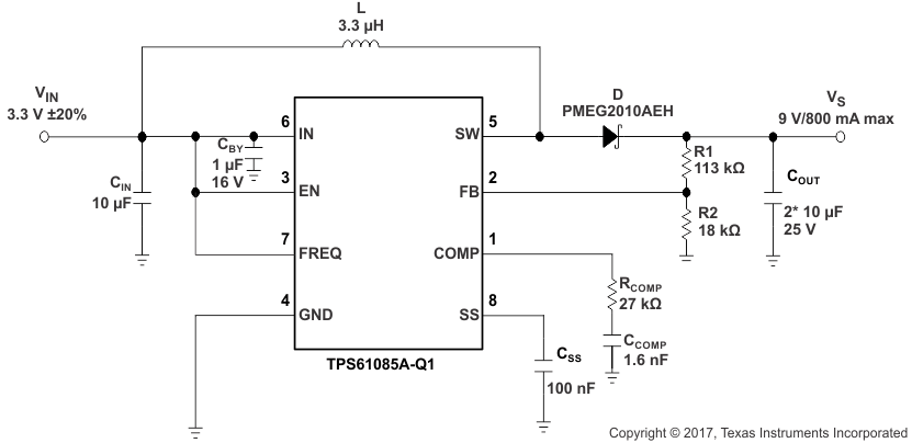 Figure 15. Typical Application, 3.3 V to 9 V (fsw = 1.2 MHz)
  Figure 16. Typical Application, 3.3 V to 9 V (fsw = 650 kHz)
 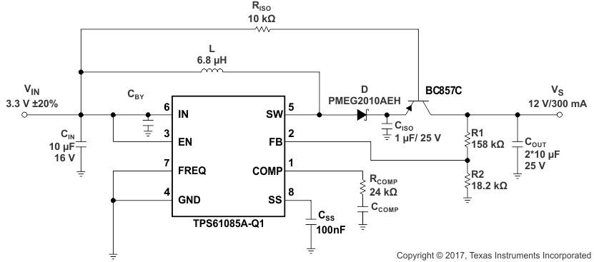 Figure 17. Typical Application With External Load Disconnect Switch
 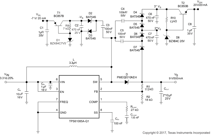 Figure 18. Typical Application 3.3 V to 9 V (fsw = 1.2 MHz) For
TFT LCD With External Charge Pumps (VGH, VGL)
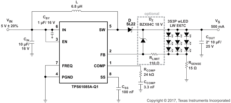 Figure 19. Simple Application (5-V Input, fsw = 650 kHz) For
wLED Supply (3S3P) (With Optional Clamping Zener Diode)
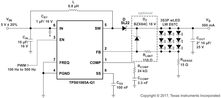 Figure 20. Simple Application (3.3-V Input, fsw = 650 kHz) For
wLED Supply (3S3P) With Adjustable Brightness Control
Using a PWM Signal on the Enable Pin
(With Optional Clamping Zener Diode)
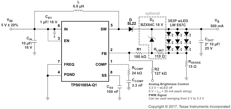 Figure 21. Simple Application (3.3-V Input, fsw = 650 kHz) For
wLED Supply (3S3P) With Adjustable Brightness Control
Using an Analog Signal on the Feedback Pin
(With Optional Clamping Zener Diode)