SLVS441D December 2002 – December 2014 TPS61042
PRODUCTION DATA.
- 1 Features
- 2 Applications
- 3 Description
- 4 Typical Application
- 5 Revision History
- 6 Pin Configuration and Functions
- 7 Specifications
- 8 Detailed Description
- 9 Application and Implementation
- 10Power Supply Recommendations
- 11Layout
- 12Device and Documentation Support
- 13Mechanical, Packaging, and Orderable Information
封装选项
请参考 PDF 数据表获取器件具体的封装图。
机械数据 (封装 | 引脚)
- DRB|8
散热焊盘机械数据 (封装 | 引脚)
- DRB|8
订购信息
7 Specifications
7.1 Absolute Maximum Ratings
over operating free-air temperature range (unless otherwise noted) (1)| MIN | MAX | UNIT | ||
|---|---|---|---|---|
| V(VIN) | Supply voltages (2) | –0.3 | 7 | V |
| V(Rs) , V(CTRL), V(FB) | Voltages | –0.3 | Vin + 0.3 | V |
| V(SW), V(LED) | Voltages(2) | 30 | V | |
| V(OVP) | Voltage | 30 | V | |
| Continuous power dissipation | See Thermal Information Table | |||
| Operating junction temperature range | –40 | 150 | °C | |
| Storage temperature, TSTG | –65 | 150 | °C | |
(1) Stresses beyond those listed under Absolute Maximum Ratings may cause permanent damage to the device. These are stress ratings only, which do not imply functional operation of the device at these or any other conditions beyond those indicated under Recommended Operating Conditions. Exposure to absolute-maximum-rated conditions for extended periods may affect device reliability.
(2) All voltage values are with respect to network ground terminal.
7.2 ESD Ratings
| VALUE | UNIT | |||
|---|---|---|---|---|
| V(ESD) | Electrostatic discharge | Human-body model (HBM), per ANSI/ESDA/JEDEC JS-001(1) | ±2000 | V |
| Charged-device model (CDM), per JEDEC specification JESD22-C101(2) | ±750 | |||
(1) JEDEC document JEP155 states that 500-V HBM allows safe manufacturing with a standard ESD control process.
(2) JEDEC document JEP157 states that 250-V CDM allows safe manufacturing with a standard ESD control process.
7.3 Recommended Operating Conditions
over operating free-air temperature range (unless otherwise noted)| MIN | TYP | MAX | UNIT | ||
|---|---|---|---|---|---|
| VI | Input voltage range | 1.8 | 6 | V | |
| Vs | Output voltage range | VIN | 27.5 | V | |
| VSW | Switch voltage | 30 | V | ||
| I(LED) | Maximum LED switch current | 60 | mA | ||
| L | Inductor(1) | 4.7 | µH | ||
| f | Switching frequency(1) | 1 | MHz | ||
| CI | Input capacitor(1) | 4.7 | µF | ||
| CO | Output capacitor(1) | 100 | nF | ||
| TA | Operating ambient temperature | –40 | 85 | °C | |
| TJ | Operating junction temperature | –40 | 125 | °C | |
(1) See application section for further information.
7.4 Thermal Information
| THERMAL METRIC(1) | TPS61042 | UNIT | |
|---|---|---|---|
| DRB PACKAGE | |||
| 8 PINS | |||
| RθJA | Junction-to-ambient thermal resistance | 48.6 | °C/W |
| RθJC(top) | Junction-to-case (top) thermal resistance | 66.9 | |
| RθJB | Junction-to-board thermal resistance | 23.8 | |
| ψJT | Junction-to-top characterization parameter | 1.5 | |
| ψJB | Junction-to-board characterization parameter | 23.9 | |
| RθJC(bot) | Junction-to-case (bottom) thermal resistance | 5.2 | |
(1) For more information about traditional and new thermal metrics, see the IC Package Thermal Metrics application report, SPRA953.
7.5 Electrical Characteristics
VI = 3.6 V, CTRL= VI, TA = -40°C to + 85°C, typical values are at TA= 25°C (unless otherwise noted)| PARAMETER | TEST CONDITIONS | MIN | TYP | MAX | UNIT | |
|---|---|---|---|---|---|---|
| SUPPLY CURRENT | ||||||
| VI | Input voltage range | 1.8 | 6.0 | V | ||
| I(Q) | Operating quiescent current into VIN | IO = 0 mA, not switching | 38 | 65 | µA | |
| IO(sd) | Shutdown current | CTRL = GND | 0.1 | 1 | µA | |
| VUVLO | Under-voltage lockout threshold | VI falling | 1.5 | 1.7 | V | |
| CTRL | ||||||
| VIH | CTRL high level input voltage | 1.3 | V | |||
| VIL | CTRL low level input voltage | 0.3 | V | |||
| IIkg | CTRL input leakage current | CTRL = GND or VIN | 0.1 | µA | ||
| ton | Minimum CTRL pulse width to enable | CTRL = low to high | 50 | µs | ||
| toff | Minimum CTRL pulse width to disable | CTRL = high to low | 10 | 32 | ms | |
| f(CTRL) | PWM switching frequency applied to CTRL | 0.1 | 50 | kHz | ||
| D(CTRL) | PWM duty cycle applied to CTRL | 1% | 100% | |||
| POWER SWITCH AND CURRENT LIMIT (SW) | ||||||
| VS | Maximum switch voltage | 30 | V | |||
| rds(ON) | MOSFET on-resistance | VI = 3.6 V; I(SW) = 200 mA | 300 | 600 | mΩ | |
| Ilkg | MOSFET leakage current | V(SW) = 28 V | 0.1 | 10 | µA | |
| ILIM | MOFSET current limit | 400 | 500 | 600 | mA | |
| LED SWITCH AND CURRENT LIMIT (LED) | ||||||
| VS | Maximum switch voltage | 30 | V | |||
| rds(ON) | MOSFET on-resistance | VI = 3.6 V; IS = 20 mA | 1 | 2 | Ω | |
| Ilkg | MOSFET leakage current | V(LED)= 28 V | 0.1 | 10 | µA | |
| OUTPUT | ||||||
| VO | Output voltage range | VI | 27.5 | V | ||
| I(FB) | Feedback input bias current(1) | V(FB) = 0.252 V | 100 | nA | ||
| VFB | Feedback trip point voltage | 1.8 V ≤ VI≤ 6 V | 244 | 252 | 260 | mV |
| V(OVP) | Output overvoltage protection | VO rising | 27.5 | 29 | 30 | V |
| Vhys(OVP) | Output overvoltage protection hysteresis | 5 | 7 | V | ||
| I(OVP) | OVP input current | VO = 15 V | 9 | 12 | µA | |
(1) The feedback input is high impedance MOSFET Gate input.
7.6 Typical Characteristics
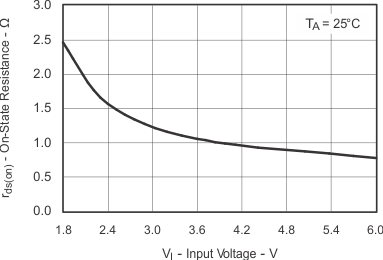
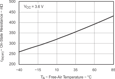
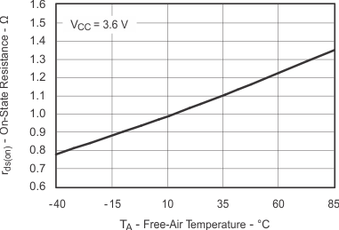
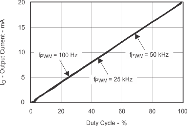
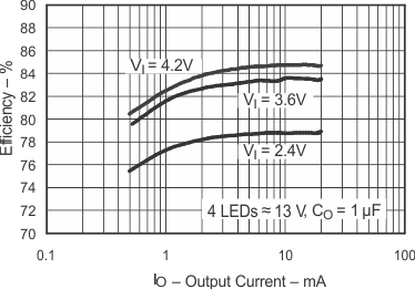
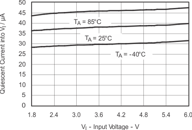
Table 1. Table of Graphs
| FIGURE | |||
|---|---|---|---|
| η | Efficiency | vs LED current | Figure 1 |
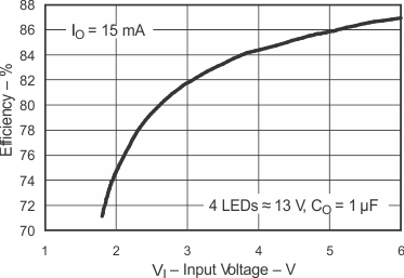
| vs Input voltage | Figure 2 | ||
| IQ | Operating Quiescent Current into VIN | vs Input voltage and Temperature | Figure 3 |
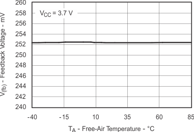
| V(FB) | Feedback voltage | vs Temperature | Figure 4 |
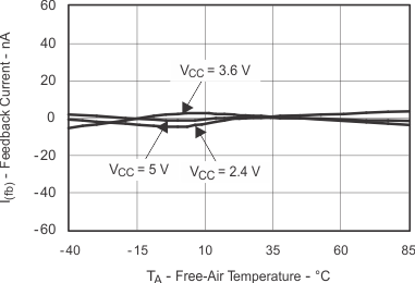
| I(FB) | Feedback current | vs Temperature | Figure 5 |
| rds(on) | Main switch Q1 | vs Temperature | Figure 6 |
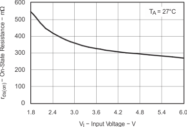
| vs Input voltage | Figure 7 | ||
| LED switch Q2 | vs Temperature | Figure 8 | |
| vs Input voltage | Figure 9 | ||
| ILED | Average LED current | vs PWM duty cycle on CTRL pin | Figure 10 |
vs Input Voltage and Temperature