SLVS441D December 2002 – December 2014 TPS61042
PRODUCTION DATA.
- 1 Features
- 2 Applications
- 3 Description
- 4 Typical Application
- 5 Revision History
- 6 Pin Configuration and Functions
- 7 Specifications
- 8 Detailed Description
- 9 Application and Implementation
- 10Power Supply Recommendations
- 11Layout
- 12Device and Documentation Support
- 13Mechanical, Packaging, and Orderable Information
封装选项
请参考 PDF 数据表获取器件具体的封装图。
机械数据 (封装 | 引脚)
- DRB|8
散热焊盘机械数据 (封装 | 引脚)
- DRB|8
订购信息
9 Application and Implementation
NOTE
Information in the following applications sections is not part of the TI component specification, and TI does not warrant its accuracy or completeness. TI’s customers are responsible for determining suitability of components for their purposes. Customers should validate and test their design implementation to confirm system functionality.
9.1 Application Information
9.1.1 Efficiency
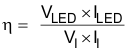
The overall efficiency of the application depends on the specific application conditions and mainly on the selection of the inductor. A lower inductor value increases the switching frequency and switching losses yielding in a lower efficiency. A lower inductor dc resistance has lower copper losses, giving a higher efficiency. Therefore, the efficiency can typically vary ±5% depending on the selected inductor. Figure 1 and Figure 2 can be used as a guideline for the application efficiency. These curves show the typical efficiency powering four LEDs using a 4.7 µH inductor with just 1,2 mm height. The efficiency curve in Figure 1 and Figure 2 show the efficiency delivering the power to the LEDs rather than the overall converter efficiency and is calculated as:
9.1.2 Setting The LED Current
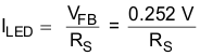
The converter regulates the LED current by regulating the voltage across the current sense resistor (RS). The voltage across the sense resistor is regulated to the internal reference voltage of V(FB) = 252 mV.
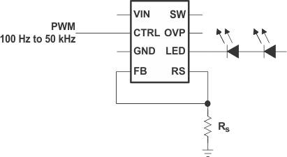 Figure 12. Setting the LED Current
The LED current can be calculated:
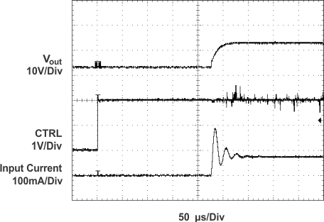
The current programming method is used when the brightness of the LEDs is fixed or controlled by a PWM signal applied to the CTRL pin. When using a PWM signal on the CTRL pin, the LED brightness is only dependent on the PWM duty cycle, independent of the PWM frequency, or amplitude, which simplifies the system.
Alternatively, an analog voltage can be used as well to control the LED brightness.
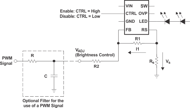 Figure 13. Setting the LED Current
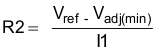
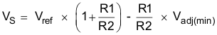
In Figure 13 the LED current is determined by the voltage applied to R2 (V(adj)) and the selection of R1, R2 and the sense resistor (RS). In this configuration, the LED current is linear controlled instead of pulsed as in the configuration before. To select the resistor values following steps are required.
- Select the voltage V(adjmax) to turn the LEDs off. → V(adjmax) (e.g. 3.3 V)
- Select the voltage V(adjmin) to turn the LEDs fully on. → V(adjmin) (e.g. 0.0 V)
- Select the maximum and minimum LED current IO(max) and IO(min). → (e.g. IO(max) = 20 mA, IO(min) = 0 mA)
- Calculate R2 to achieve a feedback current in the range of I1 = 3 µA to 10 µA as the LEDs are fully turned on:
- Calculation of R1
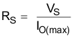
- Calculation of the sense voltage (VS) at maximum LED current
- Calculation of the required sense resistor (RS)

9.1.3 PWM Control With Separate Enable
The control pin (CTRL) combines the enable function as well as the PWM brightness control function in one pin. For some systems an independent enable function is required. One way to implement this is to use the brightness control configuration as shown in the previous section Figure 13.
Other possible solutions are shown in Figure 14, Figure 15, Figure 16.
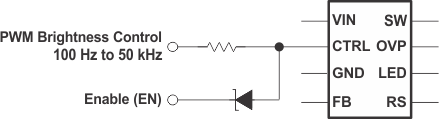 Figure 14. Separate Enable and PWM Control Using a Schottky Diode
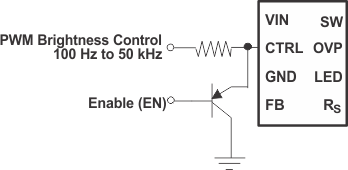 Figure 15. Separate Enable and PWM Control Using a Transistor
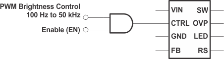 Figure 16. Separate Enable and PWM Control Using an AND Gate
9.1.4 Example Schematics
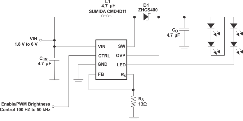 Figure 17. TPS61042 With Low LED Ripple Current and Higher Accuracy Using a 4.7 µF Output Capacitor
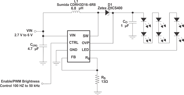 Figure 18. TPS61042 Powering 6 LEDs, Efficiency = 84%@VI = 3.6 V/19 mA
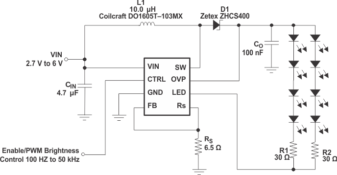 Figure 19. TPS61042 Powering 8 LEDs, Efficiency = 81%@VI = 3.6 V/18.6 mA
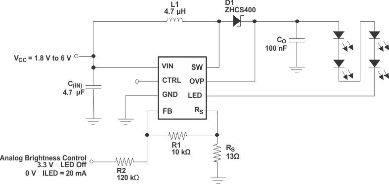 Figure 20. Adjustable Brightness Control Using an Analog Voltage
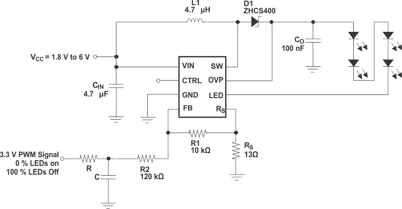 Figure 21. Alternative Adjustable Brightness Control Using PWM Signal
9.2 Typical Application
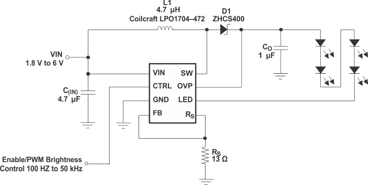 Figure 22. TPS61042 With 1,0 mm Total System Height. Efficiency = 82.7%@VI = 3.0 V/19 mA
9.2.1 Design Requirements
Table 2. Design Parameters
| DESIGN PARAMETER | Typical VALUE |
|---|---|
| Input Voltage | 1.8 V to 6 V |
| Output Voltage | VIN to 27.5 V |
| Dimming frequency | 0.1 to 50 kHz |
9.2.2 Detailed Design Procedure
9.2.2.1 Inductor Selection, Maximum Load Current, and Switching Frequency
The PFM peak current control scheme of the TPS61042 is inherently stable. The inductor value does not affect the stability of the regulator. The selection of the inductor together with the nominal LED current, input, and output voltage of the application determines the switching frequency of the converter.
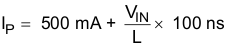
The first step is to calculate the maximum load current the converter can support using the selected inductor. The inductor value has less effect on the maximum available load current and is only of secondary order. A good inductor value to start with is 4.7 µH. Depending on the application, inductor values down to 1.0 µH can be used. The maximum inductor value is determined by the maximum on time of the switch of 6 µs (typ). The peak current limit of 500 mA (typ) must be reached within this 6 µs for proper operation. The maximum load current of the converter is determined at the operation point where the converter starts to enter the continuous conduction mode. The converter must always operate in discontinuous conduction mode to maintain regulation.
Depending on the time period of the inductor current fall time being larger or smaller compared to the minimum off time of the converter (400ns typ), the maximum load current can be calculated.
Inductor fall time:
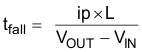
For tfall ≥ 400 ns
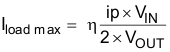
for tfall ≤ 400 ns
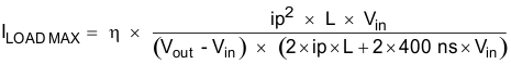
with:
L = selected inductor value
η = expected converter efficiency. Typically between 70% to 85%
(Peak inductor current as described in the peak current control section)
The above formula contains the expected converter efficiency that allows calculating the expected maximum load current the converter can support. The efficiency can be taken out of the efficiency graphs shown in Figure 1 and Figure 2 or 80% can be used as an accurate estimation.
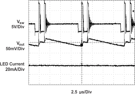
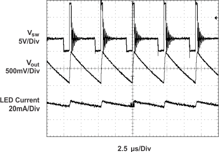
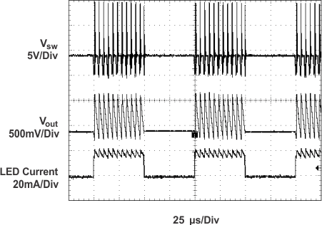
If the converter can support the desired LED current, the next step is to calculate the converter switching frequency at the operation point, which must be ≤1 MHz. Also the converter switching frequency should be much higher than the applied PWM frequency at the CTRL pin to avoid non-linear brightness control. Assuming the converter shows no double pulses or pulse bursts (Figure 24, Figure 25) on the switch node (SW) the switching frequency at the operation point can be calculated as:
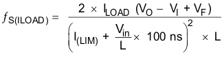
with:
I(LIM) = minimum switch current limit (500 mA typ)
L = selected inductor value
I(LOAD) = nominal load or LED current
VF = Rectifier diode forward voltage (typically 0.3 V)
The smaller the inductor value, the higher the switching frequency of the converter but the lower the efficiency.
The selected inductor must have a saturation current that meets the maximum peak current of the converter as calculated in the peak current control section. Use the maximum value for I(LIM) (600mA) for this calculation.
Another important inductor parameter is the DC resistance. The lower the DC resistance the higher the efficiency of the converter. See Table 3 and Figure 22 to Figure 21 for inductor selection.
Table 3. Possible Inductor(1)
| INDUCTOR VALUE | COMPONENT SUPPLIER | SIZE |
|---|---|---|
| 10 µH | muRata LQH43CN100K01 | 4,5 mm×3,2 mm×2.6 mm |
| 4.7 µH | muRata LQH32CN4R7M11 | 3,2 mm×2,5 mm×2,0 mm |
| 10 µH | Coilcraft DO1605T-103MX | 5,5 mm ×4,1 mm ×1,8 mm |
| 4.7 µH | Sumida CDRH3D16-4R7 | 3,8 mm×3,8 mm×1,8 mm |
| 3.3 µH | Sumida CMD4D11- 3R3 | 3,5 mm×5,3 mm×1,2 mm |
| 4.7 µH | Sumida CMD4D11- 4R7 | 3,5 mm×5,3 mm×1,2 mm |
| 3.3 µH | Sumida CMD4D11- 3R3 | 3,5 mm×5,3 mm×1,2 mm |
| 4.7 µH | Coiltronics SD12-4R7 | 5,2 mm×5,2 mm×1,2 mm |
| 3.3 µH | Coilcraft LPO1704-332M | 6,6 mm×5,5 mm×1,0 mm |
| 4.7 µH | Coilcraft LPO1704-472M | 6,6 mm×5,5 mm×1,0 mm |
9.2.2.2 Output Capacitor Selection and Line Regulation
For better output voltage filtering, a low ESR output capacitor is recommended. Ceramic capacitors have a low ESR value, but depending on the application, tantalum capacitors can be used.
The selection of the output capacitor value directly influences the output voltage ripple of the converter which also influences line regulation. The larger the output voltage ripple, the larger the line regulation, which means that the LED current changes if the input voltage changes. If a certain change in LED current gives a noticeable change in LED brightness, depends on the LED manufacturer and on the application. Applications requiring good line regulation ≤1%/V (typ) must use output capacitor values ≥1 µF.
See Table 3 and Figure 22 to Figure 21 for the selection of the output capacitor.
Assuming the converter does not show double pulses or pulse bursts on the switch node (SW), the output voltage ripple is calculated as (see Figure 24, Figure 25):
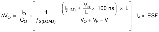
with:
I(LIM) = minimum switch current limit (400 mA typ)
L = selected inductor value
I(LOAD) = nominal load current
ƒS = switching frequency at the nominal load current as calculated before.
VF = rectifier diode forward voltage (0.3 V typ)
CO = selected output capacitor
ESR = output capacitor ESR value
9.2.2.3 Input Capacitor Selection
For good input voltage filtering, low ESR ceramic capacitors are recommended. A 4.7 µF ceramic input capacitor is sufficient for most applications. For better input voltage filtering the capacitor value can be increased. Refer to Table 2 and Figure 22 to Figure 21 for input capacitor selection.
Table 4. Possible Input and Output Capacitors(1)
| CAPACITOR | VOLTAGE RATING | COMPONENT SUPPLIER | COMMENTS |
|---|---|---|---|
| 4.7 µF/X5R/0805 | 6.3 V | Tayo Yuden JMK212BY475MG | CI |
| 10 µF/X5R/0805 | 6.3 V | Tayo Yuden JMK212BJ106MG | CI |
| 100 nF | Any | CO | |
| 220 nF | Any | CO | |
| 470 nF | Any | CO | |
| 1.0 µF/X7R/1206 | 25 V | Tayo Yuden TMK316BJ105KL | CO |
| 1.0 µF/X7R/1206 | 35 V | Tayo Yuden GMK316BJ105KL | CO |
| 4.7 µF/X5R/1210 | 25 V | Tayo Yuden TMK325BJ475MG | CO |
9.2.2.4 Diode Selection
To achieve high efficiency, a Schottky diode must be used. The current rating of the diode must meet the peak current rating of the converter as it is calculated in the peak current control section. Use the maximum value for I(Lim) for this calculation. See Table 5 and Figure 22 to Figure 21 for the Schottky diode selection.
Table 5. Possible Diodes(1)
| COMPONENT SUPPLIER | REVERSE VOLTAGE |
|---|---|
| ON Semiconductor MBR0530 | 30 V |
| ON Semiconductor MBR0520 | 20 V |
| Toshiba CRS02 | 30 V |
| Zetex ZHCS400 | 40 V |
9.2.3 Application Curves