SLVS441D December 2002 – December 2014 TPS61042
PRODUCTION DATA.
- 1 Features
- 2 Applications
- 3 Description
- 4 Typical Application
- 5 Revision History
- 6 Pin Configuration and Functions
- 7 Specifications
- 8 Detailed Description
- 9 Application and Implementation
- 10Power Supply Recommendations
- 11Layout
- 12Device and Documentation Support
- 13Mechanical, Packaging, and Orderable Information
封装选项
请参考 PDF 数据表获取器件具体的封装图。
机械数据 (封装 | 引脚)
- DRB|8
散热焊盘机械数据 (封装 | 引脚)
- DRB|8
订购信息
11 Layout
11.1 Layout Guidelines
In all switching power supplies the layout is an important step in the design, especially at high peak currents and switching frequencies. If the layout is not carefully done, the regulator might show noise problems and duty cycle jitter.
The input capacitor should be placed as close as possible to the input pin for good input voltage filtering. The inductor and diode must be placed as close as possible to the switch pin to minimize noise coupling into other circuits. Since the feedback pin and network is a high impedance circuit, the feedback network should be routed away from the inductor.
11.2 Layout Example
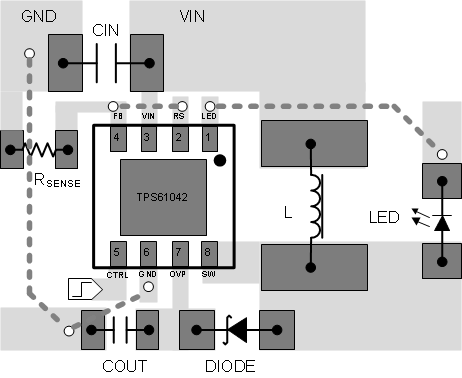 Figure 27. Layout Example
11.2.1 Thermal Considerations
The TPS61042 comes in a thermally enhanced QFN package. The package includes a thermal pad improving the thermal capabilities of the package. See the QFN/SON PCB Attachment application note (SLUA271).
The thermal resistance junction to ambient RΘJA of the QFN package greatly depends on the PCB layout. Using thermal vias and wide PCB traces improves the thermal resistance RΘJA. Under normal operation conditions no PCB vias are required for the thermal pad. However, the thermal PowerPAD™ must be soldered to the PCB.