SLVS273A February 2000 – November 2015 TPS60140 , TPS60141
PRODUCTION DATA.
- 1 Features
- 2 Applications
- 3 Description
- 4 Revision History
- 5 Description (continued)
- 6 Device Comparison Table
- 7 Pin Configuration and Functions
- 8 Specifications
- 9 Detailed Description
- 10Application and Implementation
- 11Power Supply Recommendations
- 12Layout
- 13Device and Documentation Support
- 14Mechanical, Packaging, and Orderable Information
9 Detailed Description
9.1 Overview
The TPS6014x devices regulate the output voltage using an improved pulse-skip topology. In pulse-skip mode the error amplifier disables switching of the power stages when it detects an output voltage higher than 5 V. The oscillator halts and the controller skips switching cycles. The error amplifier reactivates the oscillator and starts switching of the power stages again when the output voltage drops below 5 V. The output resistance of the charge pump is controlled to improve the ripple performance. This limits the output current to the minimum that is necessary to sustain a regulated output voltage. The benefit is that the ripple performance is nearly as good as with a linear-regulation topology.
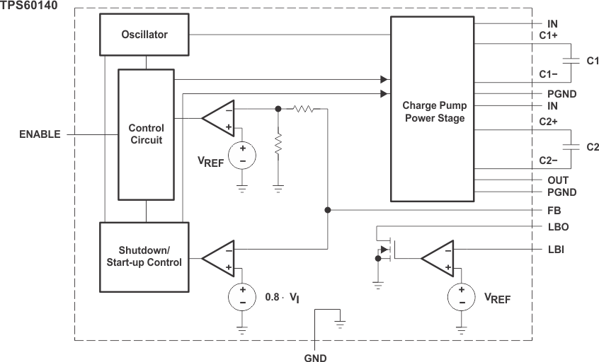
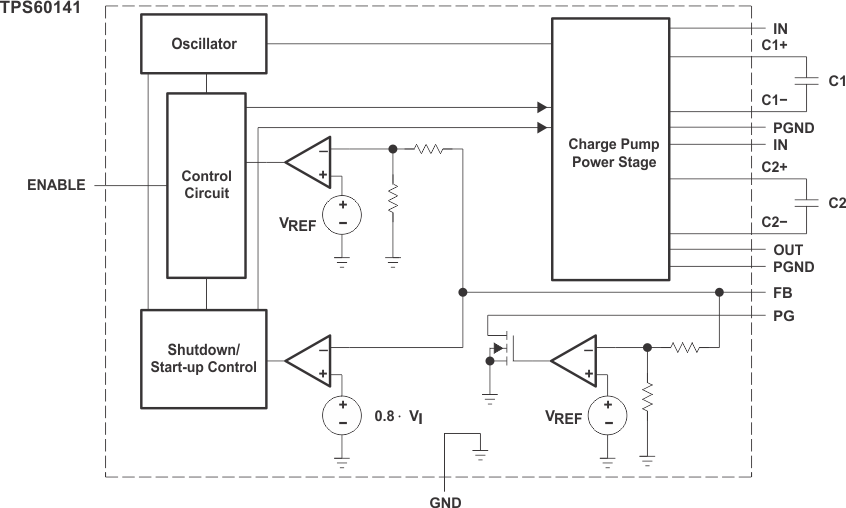
At light loads a conventional pulse-skip regulation mode is used, but the charge pump output resistance is held at a high level. The pulse-skip regulation minimizes the operating current because the charge pump does not switch continuously and hence the gate-charge losses of the MOSFETs are reduced. Additionally, all functions except voltage reference, error amplifier, and low-battery or power-good comparator are deactivated when the output is higher than 5 V. When switching is disabled by the error amplifier, the load is also isolated from the input. This improved pulse-skip control topology is also referred to as active-cycle control.
9.2 Functional Block Diagrams
 Figure 3. TPS60140 Functional Block Diagram
 Figure 4. TPS60141 Functional Block Diagram
9.3 Feature Description
9.3.1 Undervoltage Lockout
The TPS6014x devices have an undervoltage lockout feature that deactivates the device and places it in shutdown mode when the input voltage falls below 1.6 V.
9.3.2 Low-Battery Detector (TPS60140 Only)
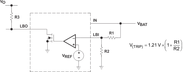
The internal low-battery comparator trips at 1.21 V ± 5% when the voltage on pin LBI ramps down. The voltage V(TRIP) at which the low battery warning is issued can be adjusted with a resistive divider as shown in Figure 5. TI recommends that the sum of resistors R1 and R2 to be in the 100-kΩ to 1-MΩ range. When choosing R1 and R2, be aware of the input leakage current into the LBI terminal.
LBO is an open-drain output. TI recommends an external pullup resistor to OUT, in the 100-kΩ to 1-MΩ range. During start-up, the LBO output signal is invalid for the first 500 µs. LBO is high impedance when the device is disabled. If the low-battery comparator function is not used, connect LBI to ground and leave LBO unconnected.
 Figure 5. Programming of the Low-Battery Comparator Trip Voltage
A 100-nF ceramic capacitor should be connected in parallel to R2 if large line transients are expected. These voltage drops can inadvertently trigger the low-battery comparator and produce a wrong low-battery warning signal at the LBO pin.
Formulas to calculate the resistive divider for low battery detection, with V(LBI) = 1.15 V to 1.27 V:


Formulas to calculate the minimum and maximum trip voltage:


Table 1. Recommended Values for the Resistive Divider From the E96 Series (±1%)
| VI/V | R1/kΩ | R2/kΩ | V(TRIP)MIN/V | V(TRIP)MAX/V |
|---|---|---|---|---|
| 1.8 | 357 | 732 | 1.700 | 1.902 |
| 1.9 | 365 | 634 | 1.799 | 2.016 |
| 2 | 412 | 634 | 1.883 | 2.112 |
| 2.1 | 432 | 590 | 1.975 | 2.219 |
| 2.2 | 442 | 536 | 2.08 | 2.338 |
9.3.3 Power-Good Detector (TPS60141)
The power-good (PG) terminal is an open-drain output that is pulled low when the output is out of regulation. When the output rises to typically 90% of its nominal voltage, the power-good output is released. Power-good is high impedance in shutdown. In normal operation an external pullup resistor must be connected between PG and OUT. The resistor should be in the 100-kΩ to 1-MΩ range. If the power-good function is not used, the PG terminal should remain unconnected.
9.4 Device Functional Modes
9.4.1 Start-Up Procedure and Shutdown
During start-up (that is, when ENABLE is set from logic low to logic high), the output capacitor is charged up with a limited current until the output voltage (VO) reaches 0.8 × VI. When the start-up comparator detects this voltage limit, the IC begins switching. This precharging of the output capacitor ensures a short start-up time. In addition, the inrush current into an empty output capacitor is limited because the current through the switches is limited before the charge pump starts switching.
Driving ENABLE low places the device in shutdown mode. This disables all switches, the oscillator, and control logic. The device typically draws 0.05 µA of supply current in this mode. Leakage current drawn from the output is as low as 1 µA (maximum). The device exits shutdown once ENABLE is set to a high level. When the device is in shutdown, the load is isolated from the input.
9.4.2 Short-Circuit Protection
The TPS6014x devices are also short-circuit protected. The output current is limited to typically 100 mA during a hard short-circuit condition at the output; that is, when VOUT is GND. In this case, the condition to enter the start-up mode is met, the device stops switching and controls the on-resistance of the appropriate MOSFET switches to limit the current.