SLVS273A February 2000 – November 2015 TPS60140 , TPS60141
PRODUCTION DATA.
- 1 Features
- 2 Applications
- 3 Description
- 4 Revision History
- 5 Description (continued)
- 6 Device Comparison Table
- 7 Pin Configuration and Functions
- 8 Specifications
- 9 Detailed Description
- 10Application and Implementation
- 11Power Supply Recommendations
- 12Layout
- 13Device and Documentation Support
- 14Mechanical, Packaging, and Orderable Information
10 Application and Implementation
NOTE
Information in the following applications sections is not part of the TI component specification, and TI does not warrant its accuracy or completeness. TI’s customers are responsible for determining suitability of components for their purposes. Customers should validate and test their design implementation to confirm system functionality.
10.1 Application Information
The TPS6014x charge pumps provide a regulated 5-V output from a 1.8-V to 3.6-V input voltage range. They can deliver a maximum continuous load current of at least 100 mA at VI = 2 V minimum.
10.2 Typical Application
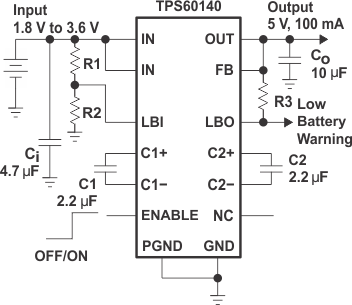 Figure 6. Typical Application Schematic
10.2.1 Design Requirements
Designed specifically for space-critical battery-powered applications, the complete charge pump circuit requires only four external capacitors. The design guideline provides a component selection to operate the device within the Recommended Operating Conditions.
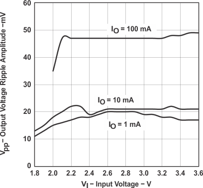
Table 2 shows the list of components for the Application Curves.
Table 2. Components for Application Curves
| REFERENCE | VALUE | DESCRIPTION | MANUFACTURER | PART NUMBER |
|---|---|---|---|---|
| C1, C2 | 2.2 µF | Ceramic flying capacitors | Taiyo Yuden | EMK316BJ225KL-T |
| CIN | 4.7 µF | Ceramic input capacitor | Taiyo Yuden | LMK316BJ475KL-T |
| COUT | 10 µF | Ceramic output capacitor | Taiyo Yuden | JMK316BJ106ML-T |
| R1 | 357 kΩ | LBI input voltage adjustment | E96-Series | |
| R2 | 619 kΩ | LBI input voltage adjustment | E96-Series | |
| R3 | 1 MΩ | Pullup resistor for the open-drain output LBO |
10.2.2 Detailed Design Procedure
10.2.2.1 Capacitor Selection
The capacitance values of the TPS6014x external capacitors are closely linked to the output current and output ripple requirements. For lowest ripple, low ESR (< 0.1 Ω) capacitors should be used at the input and output of the charge pump.
The input capacitor improves system efficiency by reducing the input impedance. It also stabilizes the input current of the power source. The input capacitor should be chosen according to the power supply used and the distance from the power source to the converter IC. The input capacitor selection also depends on the output ripple requirements. CIN is recommended to be about 2-times to 4-times as large as the flying capacitors. The lower the ESR of the input capacitor CIN, the lower is the output ripple.
The output capacitor COUT can be selected from 2× to 50× larger than the flying capacitor, depending on the ripple tolerance. The larger COUT and the lower its ESR, the lower will be the output voltage ripple.
Generally, the flying capacitors will be the smallest. Only ceramic capacitors are recommended because of their low ESR and because they retain their capacitance at the switching frequency. Be aware that, depending on the material used to manufacture them, ceramic capacitors might lose their capacitance over temperature and voltage. Ceramic capacitors of type X7R or X5R material will keep their capacitance over temperature and voltage, whereas Z5U or Y5V-type capacitors will decrease in capacitance. Table 3 lists recommended capacitor values.
Table 3. Recommended Capacitor Values
| IOUT
(mA) |
CIN
(µF) |
C(xF)
(µF) |
COUT
(µF) |
VPPTYP (mV) |
|---|---|---|---|---|
| 0 − 50 | 4.7 | 2.2 | 4.7 | 40 |
| 0 − 100 | 4.7 | 2.2 | 10 | 40 |
| 0 − 100 | 4.7 | 2.2 | 22 | 18 |
If the measured output voltage ripple is too high for the application, improvements can be made. The first step is to increase the capacitance at the output. If the ripple is still too high, the second step would be to increase the capacitance at the input. For lower output currents, lower value flying capacitors can be used. Table 3 and Table 4 lists the manufacturers of recommended capacitors.
Table 4. Recommended Capacitors(1)
| MANUFACTURER | PART NUMBER | CAPACITANCE | CASE SIZE | TYPE |
|---|---|---|---|---|
| Taiyo Yuden | LMK212BJ105KG−T EMK316BJ225KL−T LMK212BJ225MG−T LMK316BJ475KL−T JMK316BJ106ML–T LMK325BJ106MN−T LMK432226MM−T |
1 µF 2.2 µF 2.2 µF 4.7 µF 10 µF 10 µF 22 µF |
805 1206 805 1206 1206 1210 1812 |
Ceramic Ceramic Ceramic Ceramic Ceramic Ceramic Ceramic |
| AVX | 0805ZC105KAT2A 1206ZC225KAT2A |
1 µF 2.2 µF |
805 1206 |
Ceramic Ceramic |
Table 5. Recommended Capacitor Manufacturers
| MANUFACTURER | CAPACITOR TYPE | INTERNET SITE |
|---|---|---|
| Taiyo Yuden | X7R/X5R ceramic | http://www.t−yuden.com/ |
| AVX | X7R/X5R ceramic | http://www.avxcorp.com/ |
10.2.3 Application Curves
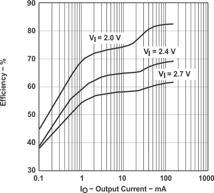
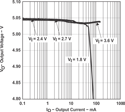
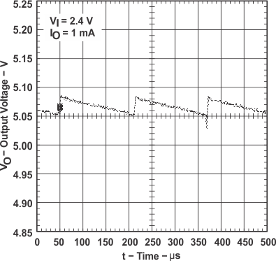
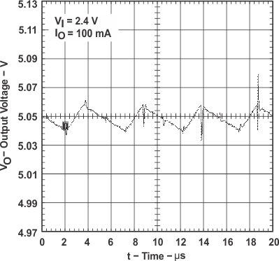
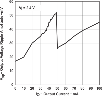
Output Current
Input Voltage
