ZHCSL72B October 2016 – July 2021 TPS57114C-Q1
PRODUCTION DATA
- 1 特性
- 2 应用
- 3 说明
- 4 Revision History
- 5 Pin Configuration and Functions
- 6 Specifications
-
7 Detailed Description
- 7.1 Overview
- 7.2 Functional Block Diagram
- 7.3 Feature Description
- 7.4
Device Functional Modes
- 7.4.1 Adjusting the Output Voltage
- 7.4.2 Enable Functionality and Adjusting Undervoltage Lockout
- 7.4.3 Slow-Start or Tracking Pin
- 7.4.4 Sequencing
- 7.4.5 Constant Switching Frequency and Timing Resistor (RT/CLK Pin)
- 7.4.6 Overcurrent Protection
- 7.4.7 Frequency Shift
- 7.4.8 Reverse Overcurrent Protection
- 7.4.9 Synchronize Using The RT/CLK Pin
- 7.4.10 Power Good (PWRGD Pin)
- 7.4.11 Overvoltage Transient Protection
- 7.4.12 Thermal Shutdown
- 7.4.13 Small-Signal Model for Loop Response
- 7.4.14 Simple Small-Signal Model for Peak-Current Mode Control
- 7.4.15 Small-Signal Model for Frequency Compensation
-
8 Application and Implementation
- 8.1 Application Information
- 8.2
Typical Application
- 8.2.1 Design Requirements
- 8.2.2
Detailed Design Procedure
- 8.2.2.1 Selecting the Switching Frequency
- 8.2.2.2 Output Inductor Selection
- 8.2.2.3 Output Capacitor
- 8.2.2.4 Input Capacitor
- 8.2.2.5 Slow-Start Capacitor
- 8.2.2.6 Bootstrap Capacitor Selection
- 8.2.2.7 Output-Voltage And Feedback-Resistor Selection
- 8.2.2.8 Compensation
- 8.2.2.9 Power-Dissipation Estimate
- 8.2.3 Application Curves
- 9 Power Supply Recommendations
- 10Layout
- 11Device and Documentation Support
- 12Mechanical, Packaging, and Orderable Information
7.4.15 Small-Signal Model for Frequency Compensation
The TPS57114C-Q1 device uses a transconductance amplifier for the error amplifier and readily supports two of the commonly used frequency-compensation circuits. Figure 7-13 shows the compensation circuits. High-bandwidth power-supply designs most likely implement Type 2 circuits using low-ESR output capacitors. In Type 2A, inclusion of one additional high-frequency pole attenuates high-frequency noise.
 Figure 7-13 Types of Frequency Compensation
The design guidelines for TPS57114C-Q1 loop compensation are as follows:
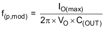
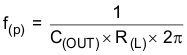
- Calculate the modulator pole, f(p,mod), and the ESR zero, f(z,mod), using Equation 14 and Equation 15. If the output voltage is a high percentage of the capacitor rating, it may be necessary to derate the output capacitor (C(OUT)). Use the manufacturer information for the capacitor to derate the capacitor value. Use Equation 16 and Equation 17 to estimate a starting point for the crossover frequency, f(c). Equation 16 is the geometric mean of the modulator pole and the ESR zero, and Equation 17 is the mean of the modulator pole and the switching frequency. Use the lower value of Equation 16 or Equation 17 as the maximum crossover frequency.
Equation 14.
 Equation 15.
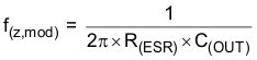 Equation 16.
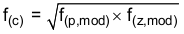 Equation 17.
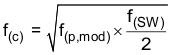
- Determine R3 by
Equation 18.
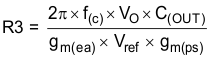
where gm(ea) is the amplifier gain (245 µS), and gm(ps) is the power-stage gain (25 S).
- Place a compensation zero at the dominant pole.
Equation 19.
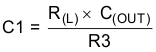
- Determine C1 by
Equation 20.
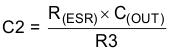
- C2 is optional. Use it, if necessary, to cancel the zero from the ESR of C(OUT).
Equation 21.