ZHCSF66B April   2016  – May 2019 TPS560200-Q1

PRODUCTION DATA.  

  1. 特性
  2. 应用
  3. 说明
    1.     Device Images
      1.      简化原理图
  4. 修订历史记录
  5. Pin Configuration and Functions
    1.     Pin Functions
  6. Specifications
    1. 6.1 Absolute Maximum Ratings
    2. 6.2 ESD Ratings
    3. 6.3 Recommended Operating Conditions
    4. 6.4 Thermal Information
    5. 6.5 Electrical Characteristics
    6. 6.6 Typical Characteristics
  7. Detailed Description
    1. 7.1 Overview
    2. 7.2 Functional Block Diagram
    3. 7.3 Feature Description
      1. 7.3.1 PWM Operation
      2. 7.3.2 PWM Frequency and Adaptive On-Time Control
      3. 7.3.3 Advanced Auto-Skip Eco-Mode Control
      4. 7.3.4 Soft-Start and Prebiased Soft-Start
      5. 7.3.5 Current Protection
      6. 7.3.6 Thermal Shutdown
    4. 7.4 Device Functional Modes
      1. 7.4.1 Normal Operation
      2. 7.4.2 Eco-Mode Operation
      3. 7.4.3 Standby Operation
  8. Application and Implementation
    1. 8.1 Application Information
    2. 8.2 Typical Application
      1. 8.2.1 Design Requirements
      2. 8.2.2 Detailed Design Procedure
        1. 8.2.2.1 Output Voltage Resistors Selection
        2. 8.2.2.2 Output Filter Selection
        3. 8.2.2.3 Input Capacitor Selection
      3. 8.2.3 Application Curves
  9. Power Supply Recommendations
  10. 10Layout
    1. 10.1 Layout Guidelines
    2. 10.2 Layout Example
  11. 11器件和文档支持
    1. 11.1 接收文档更新通知
    2. 11.2 社区资源
    3. 11.3 商标
    4. 11.4 静电放电警告
    5. 11.5 Glossary
  12. 12机械、封装和可订购信息

封装选项

机械数据 (封装 | 引脚)
散热焊盘机械数据 (封装 | 引脚)
订购信息

Application Curves

VIN = 12 V, VOUT = 1.05 V, TA = 25°C (unless otherwise noted).
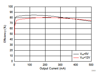
TPS560200-Q1 D003_SLVSCW4.gifFigure 8. Efficiency
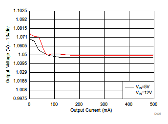
TPS560200-Q1 D005_SLVSCW4.gifFigure 10. Load Regulation
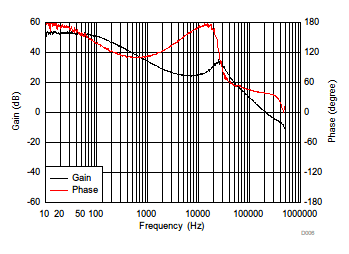
TPS560200-Q1 D006_SLVSCW4.gifFigure 12. Loop Response, IOUT = 0.25 A
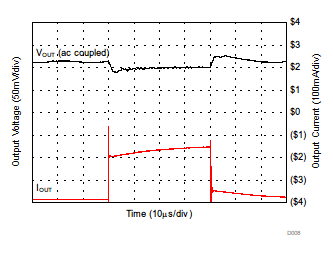
TPS560200-Q1 D008_SLVSCW4.gifFigure 14. Transient Response, 2% to 50% Load Step
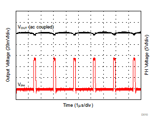
TPS560200-Q1 D010_SLVSCW4.gifFigure 16. Output Ripple, IOUT = 500 mA
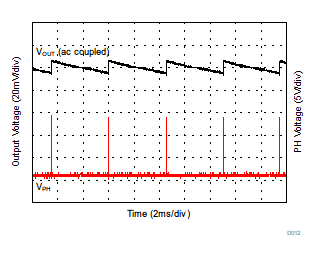
TPS560200-Q1 D012_SLVSCW4.gifFigure 18. Output Ripple, IOUT = 0 mA
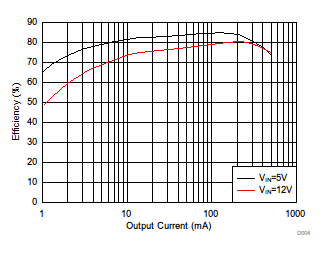
TPS560200-Q1 D004_SLVSCW4.gifFigure 9. Light-Load Efficiency
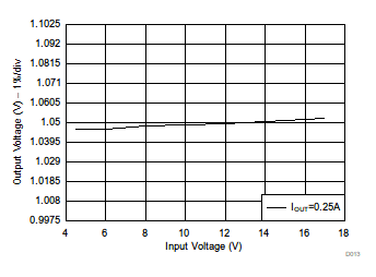
TPS560200-Q1 D013_SLVSCW4.gifFigure 11. Line Regulation
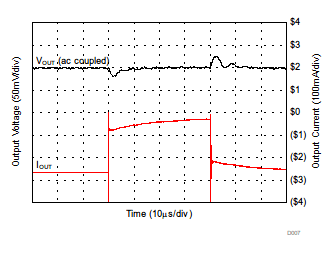
TPS560200-Q1 D007_SLVSCW4.gifFigure 13. Transient Response, 25% to 75% Load Step
TPS560200-Q1 D009_SLVSCW4.gifFigure 15. Start-Up Relative to EN
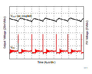
TPS560200-Q1 D011_SLVSCW4.gifFigure 17. Output Ripple, IOUT = 30 mA