ZHCSAH1B November 2012 – April 2019 TPS53819A
PRODUCTION DATA.
- 1 特性
- 2 应用
- 3 说明
- 4 修订历史记录
- 5 Pin Configuration and Functions
- 6 Specifications
-
7 Detailed Description
- 7.1 Overview
- 7.2 Functional Block Diagram
- 7.3
Feature Description
- 7.3.1 Enable and Soft-Start
- 7.3.2 Adaptive On-Time Control
- 7.3.3 Zero Crossing Detection
- 7.3.4 Output Discharge Control
- 7.3.5 Low-Side Driver
- 7.3.6 High-Side Driver
- 7.3.7 Power Good
- 7.3.8 Current Sense and Overcurrent Protection
- 7.3.9 Overvoltage and Undervoltage Protection
- 7.3.10 Out-of-Bound Protection
- 7.3.11 UVLO Protection
- 7.3.12 Thermal Shutdown
- 7.4 Device Functional Modes
- 7.5 Programming
- 7.6
Register Maps
- 7.6.1 OPERATION [01h] (R/W Byte)
- 7.6.2 ON_OFF_CONFIG [02h] (R/W Byte)
- 7.6.3 WRITE_PROTECT [10h] (R/W Byte)
- 7.6.4 CLEAR_FAULTS [03h] (Send Byte)
- 7.6.5 STORE_DEFAULT_ALL [11h] (Send Byte)
- 7.6.6 RESTORE_DEFAULT_ALL [12h] (Send Byte)
- 7.6.7 STATUS_WORD [79h] (Read Word)
- 7.6.8 CUSTOM_REG (MFR_SPECIFIC_00) [D0h] (R/W Byte)
- 7.6.9 DELAY_CONTROL (MFR_SPECIFIC_01) [D1h] (R/W Byte)
- 7.6.10 MODE_SOFT_START_CONFIG (MFR_SPECIFIC_02) [D2h] (R/W Byte)
- 7.6.11 FREQUENCY_CONFIG (MFR_SPECIFIC_03) [D3h] (R/W Byte)
- 7.6.12 VOUT_ADJUSTMENT (MFR_SPECIFIC_04) [D4h] (R/W Byte)
- 7.6.13 Output Voltage Fine Adjustment Soft Slew Rate
- 7.6.14 VOUT_MARGIN (MFR_SPECIFIC_05) [D5h] (R/W Byte)
- 7.6.15 Output Voltage Margin Adjustment Soft-Slew Rate
- 7.6.16 UVLO_THRESHOLD (MFR_SPECIFIC_06) [D6h]
-
8 Application and Implementation
- 8.1 Application Information
- 8.2
Typical Application
- 8.2.1 Design Requirements
- 8.2.2
Detailed Design Procedure
- 8.2.2.1 Custom Design With WEBENCH® Tools
- 8.2.2.2 Switching Frequency
- 8.2.2.3 Inductor (L1)
- 8.2.2.4 Output Capacitors (C10, C11, C12, C13, C14)
- 8.2.2.5 Input Capacitors (C1, C2, C3, C4, C5)
- 8.2.2.6 MOSFET (Q1, Q2)
- 8.2.2.7 VREG Bypass Capacitor (C18)
- 8.2.2.8 VDD Bypass Capacitor (C19)
- 8.2.2.9 VBST Capacitor (C7)
- 8.2.2.10 Snubber (C8 and R9)
- 8.2.2.11 Feedback Resistance, RFBH and RFBL (R17 and R18)
- 8.2.2.12 Overcurrent Limit (OCL) Setting Resistance (R10)
- 8.2.2.13 PMBus Device Address (R3 and R4)
- 8.2.2.14 PGOOD Pullup Resistor (R2)
- 8.2.2.15 SCL and SDA Pulldown Resistors (R14 and R15)
- 8.2.2.16 PMBus Pullup Resistors
- 8.2.3 Application Curves
- 9 Power Supply Recommendations
- 10Layout
- 11器件和文档支持
- 12机械、封装和可订购信息
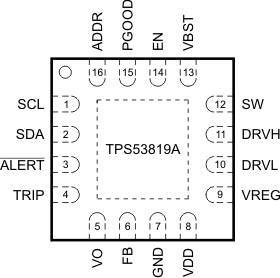
5 Pin Configuration and Functions
RGT Package
16 Pin QFN
Top View

Pin Functions
| PIN | I/O(1) | DESCRIPTION | |
|---|---|---|---|
| NAME | NO. | ||
| ADDR | 16 | I | PMBus address configuration. Connect this pin to a resistor divider between VREG and GND to program different address settings. (See Table 2 for details.) |
| ALERT | 3 | O | Open-drain alert output for the PMBus interface. |
| DRVH | 11 | O | High-side MOSFET floating driver output that is referenced to SW node. The gate drive voltage is defined by the voltage across bootstrap capacitor between VBST and SW. |
| DRVL | 10 | O | Synchronous MOSFET driver output that is referenced to GND. The gate drive voltage is defined by VREG voltage. |
| EN | 14 | I | Enable pin that can turn on the DC/DC switching converter. EN pin works in conjunction with the CP bit in PMBus ON_OFF_CONFIG register. |
| FB | 6 | I | Output voltage feedback input. Connect this pin to a resistor divider between output voltage and GND. |
| GND | 7 | G | Ground pin. |
| PGOOD | 15 | O | Open drain power good status signal. Provides start-up delay time after FB voltage falls within specified limits. After FB voltage goes out of specified limits, PGOOD goes low within 2 µs. |
| SCL | 1 | I | Clock input for the PMBus interface. |
| SDA | 2 | I/O | Data I/O for the PMBus interface. |
| SW | 12 | P | Output switching terminal of power converter. Connect this pin to the output inductor. |
| TRIP | 4 | I/O | OCL detection threshold setting pin. A 10-µA current with a TC of 4700ppm/°C is sourced out of the TRIP pin and is used to set the OCL trip voltage as follows:
VOCL= VTRIP/8 and ( VTRIP ≤ 3 V, VOCL ≤ 375 mV) |
| VBST | 13 | P | Supply rail for high-side gate driver (boost terminal). Connect bootstrap capacitor from this pin to SW node. Internally connected to VREG via bootstrap PMOS switch. |
| VDD | 8 | P | Controller power supply input. |
| VO | 5 | I | Output voltage. |
| VREG | 9 | P | 5-V low-drop-out (LDO) output. Supplies the internal analog and driver circuitry. |
(1) I=Input, O=Output, P=Power, G=Ground