ZHCS979G June 2012 – November 2025 TPS53318 , TPS53319
PRODUCTION DATA
7.3.2 自适应导通时间 D-CAP™ 集成电路控制和频率选择
TPS53318 和 TPS53319 器件都没有用来确定开关频率的专用振荡器。但是,这些器件通过将输入和输出电压前馈至导通时间单次触发计时器,实现了伪恒定频率运行。自适应导通时间控制功能可将导通时间调整为与输入电压成反比,并与输出电压成正比,如方程式 1 所示。
方程式 1. 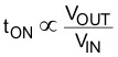
这样可使开关频率在宽输入电压范围内稳态条件下保持相当恒定。开关频率可通过连接在 RF 引脚和 GND 之间或 RF 引脚和 VREG 引脚之间的电阻器从八个预设值中进行选择,如表 7-1 所示。保持开路电阻会将开关频率设置为 500kHz。
表 7-1 电阻和开关频率
| 电阻 (RRF) 连接 | 开关频率 (fSW) (kHz) | |
|---|---|---|
| 值 (kΩ) | 连接到 | |
| 0 | GND | 250 |
| 187 | GND | 300 |
| 619 | GND | 400 |
| 断开 | 不适用 | 500 |
| 866 | VREG | 600 |
| 309 | VREG | 750 |
| 124 | VREG | 850 |
| 0 | VREG | 970 |
关断时间由 PWM 比较器调制。VFB 节点电压(电阻分压器的中点)与附带斜坡信号的 0.6V 内部基准电压进行比较。当两个信号匹配时,PWM 比较器将发出一个置位信号,以终止关断时间(关断低侧 MOSFET 并导通高侧 MOSFET)。如果电感器电流电平低于 OCP 阈值,则置位信号有效,否则关断时间会延长,直到电流电平降至低于阈值。
图 7-2 中显示的波形显示了无斜坡补偿的导通时间控制。图 7-3 中显示的波形显示了无斜坡补偿的导通时间控制。
 图 7-2 无斜坡补偿的导通时间控制
 图 7-3 有斜坡补偿的导通时间控制