ZHCS979G June 2012 – November 2025 TPS53318 , TPS53319
PRODUCTION DATA
7.3.12 小信号模型
根据小信号环路分析,使用 D-CAP 集成电路模式的降压转换器可以简化为如图 7-4 所示。
 图 7-4 简化调制器模型
输出电压与内部基准电压进行比较(为求简化,此处忽略斜坡信号)。PWM 比较器确定导通高侧 MOSFET 的时间。可以假定比较器的增益和速度足够高,可使每个导通周期开始时的电压基本保持恒定。
方程式 6. 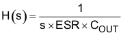
为了实现环路稳定,下面定义的 0dB 频率 ƒ0 需要低于开关频率的 1/4。
方程式 7. 
根据方程式 7,D-CAP 集成电路模式调制器的环路稳定性主要取决于电容器的化学特性。例如,专用聚合物电容器 (SP-CAP) 的输出电容约为几百微法,ESR 则在 10mΩ 范围内。这些使 ƒ0 约为 100kHz 或更低,从而创建稳定的环路。但是,陶瓷电容器的 ƒ0 超过 700kHz,在与此调制器配合使用时需要特别小心。节 7.3.13中介绍了陶瓷电容器的应用电路。