ZHCSHF4J May 2004 – January 2018 TPS51116
PRODUCTION DATA.
- 1 特性
- 2 应用
- 3 说明
- 4 修订历史记录
- 5 Pin Configuration and Functions
- 6 Specifications
-
7 Detailed Description
- 7.1 Overview
- 7.2 Functional Block Diagram
- 7.3
Feature Description
- 7.3.1 VDDQ SMPS, Light Load Condition
- 7.3.2 Low-Side Driver
- 7.3.3 High-Side Driver
- 7.3.4 Current Sensing Scheme
- 7.3.5 PWM Frequency and Adaptive On-Time Control
- 7.3.6 VDDQ Output Voltage Selection
- 7.3.7 VTT Linear Regulator and VTTREF
- 7.3.8 Controling Outputs Using the S3 and S5 Pins
- 7.3.9 Soft-Start Function and Powergood Status
- 7.3.10 VDDQ and VTT Discharge Control
- 7.3.11 Current Protection for VDDQ
- 7.3.12 Current Protection for VTT
- 7.3.13 Overvoltage and Undervoltage Protection for VDDQ
- 7.3.14 Undervoltage Lockout (UVLO) Protection, V5IN (PWP), V5FILT (RGE)
- 7.3.15 Input Capacitor, V5IN (PWP), V5FILT (RGE)
- 7.3.16 Thermal Shutdown
- 7.4 Device Functional Modes
- 8 Application and Implementation
- 9 Power Supply Recommendations
- 10Layout
- 11器件和文档支持
- 12机械、封装和可订购信息
封装选项
请参考 PDF 数据表获取器件具体的封装图。
机械数据 (封装 | 引脚)
- RGE|24
- PWP|20
散热焊盘机械数据 (封装 | 引脚)
订购信息
7.4.2 Current Mode Operation
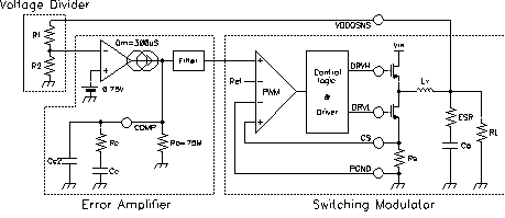
A buck converter using current mode operation can be partitioned into three portions, a voltage divider, an error amplifier and a switching modulator. By linearizing the switching modulator, we can derive the transfer function of the whole system. Because current mode scheme directly controls the inductor current, the modulator can be linearized as shown in Figure 36.
 Figure 36. Linearizing the Modulator
In this example, the inductor is located inside the local feedback loop and its inductance does not appear in the small signal model. As a result, a modulated current source including the power inductor can be modeled as a current source with its transconductance of 1/RS and the output capacitor represent the modulator portion. This simplified model is applicable in the frequency space up to approximately a half of the switching frequency. One note is, although the inductance has no influence to small signal model, it has influence to the large signal model as it limits slew rate of the current source. This means the buck converter’s load transient response, one of the large signal behaviors, can be improved by using smaller inductance without affecting the loop stability.
Equation 6 describes the total open loop transfer function of the entire system.

Assuming RL>>ESR, RO>>RC and CC>>CC2, each transfer function of the three blocks is shown starting with Equation 7.


There are three poles and two zeros in H(s). Each pole and zero is given by the following five equations.


Usually, each frequency of those poles and zeros is lower than the 0 dB frequency, f0. However, the f0 should be kept under 1/3 of the switching frequency to avoid effect of switching circuit delay. Equation 15calculates the 0 dB frequency, f0.
