SLVSA82F March 2011 – December 2014 TPS43330-Q1 , TPS43332-Q1
PRODUCTION DATA.
- 1 Features
- 2 Applications
- 3 Description
- 4 Revision History
- 5 Device Comparison Table
- 6 Pin Configuration and Functions
- 7 Specifications
-
8 Detailed Description
- 8.1 Overview
- 8.2 Functional Block Diagram
- 8.3 Feature Description
- 8.4 Device Functional Modes
-
9 Application and Implementation
- 9.1 Application Information
- 9.2
Typical Application
- 9.2.1 Design Requirements
- 9.2.2
Detailed Design Procedure
- 9.2.2.1 Boost Component Selection
- 9.2.2.2 Boost Maximum Input Current IIN_MAX
- 9.2.2.3 Boost Inductor Selection, L
- 9.2.2.4 Inductor Ripple Current, IRIPPLE
- 9.2.2.5 Peak Current in Low-Side FET, IPEAK
- 9.2.2.6 Right Half-Plane Zero RHP Frequency, fRHP
- 9.2.2.7 Output Capacitor, COUTx
- 9.2.2.8 Bandwidth of Boost Converter, fC
- 9.2.2.9 Output Ripple Voltage Due to Load Transients, ∆VOUTx
- 9.2.2.10 Selection of Components for Type II Compensation
- 9.2.2.11 Input Capacitor, CIN
- 9.2.2.12 Output Schottky Diode D1 Selection
- 9.2.2.13 Low-Side MOSFET (BOT_SW3)
- 9.2.2.14 BuckA Component Selection
- 9.2.2.15 Inductor Selection L
- 9.2.2.16 Inductor Ripple Current IRIPPLE
- 9.2.2.17 Output Capacitor COUTA
- 9.2.2.18 Bandwidth of Buck Converter fC
- 9.2.2.19 Selection of Components for Type II Compensation
- 9.2.2.20 Resistor Divider Selection for Setting VOUTA Voltage
- 9.2.2.21 BuckB Component Selection
- 9.2.2.22 Resistor Divider Selection for Setting VOUT Voltage
- 9.2.2.23 BuckX High-Side and Low-Side N-Channel MOSFETs
- 9.2.3 Application Curves
- 10Power Supply Recommendations
- 11Layout
- 12Device and Documentation Support
- 13Mechanical, Packaging, and Orderable Information
6 Pin Configuration and Functions
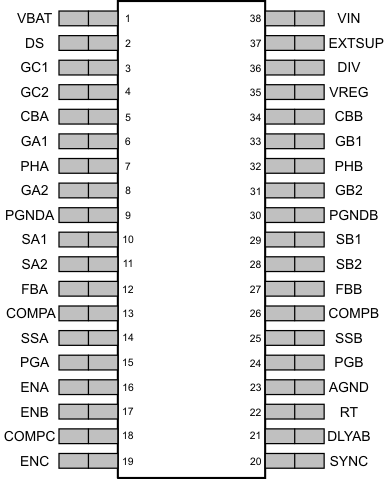
Pin Functions
| PIN | I/O | DESCRIPTION | |
|---|---|---|---|
| NAME | NO. | ||
| AGND | 23 | O | Analog ground reference |
| CBA | 5 | I | A capacitor on this pin acts as the voltage supply for the high-side N-channel MOSFET gate-drive circuitry in buck controller BuckA. When the buck is in a dropout condition, the device automatically reduces the duty cycle of the high-side MOSFET to approximately 95% on every fourth cycle to allow the capacitor to recharge. |
| CBB | 34 | I | A capacitor on this pin acts as the voltage supply for the high-side N-channel MOSFET gate-drive circuitry in buck controller BuckB. When the buck is in a dropout condition, the device automatically reduces the duty cycle of the high-side MOSFET to approximately 95% on every fourth cycle to allow the capacitor to recharge. |
| COMPA | 13 | O | Error amplifier output of BuckA and compensation node for voltage-loop stability. The voltage at this node sets the target for the peak current through the inductor of BuckA. Clamping this voltage on the upper and lower ends provides current-limit protection for the external MOSFETs. |
| COMPB | 26 | O | Error amplifier output of BuckB and compensation node for voltage-loop stability. The voltage at this node sets the target for the peak current through the inductor of BuckB. Clamping this voltage on the upper and lower ends provides current-limit protection for the external MOSFETs. |
| COMPC | 18 | O | Error-amplifier output and loop-compensation node of the boost regulator |
| DIV | 36 | I | The status of this pin defines the output voltage of the boost regulator. A high input regulates the boost converter at 11 V, a low input sets the value at 7 V, and a floating pin sets 10 V.(1) |
| DLYAB | 21 | O | The capacitor at the DLYAB pin sets the power-good delay interval used to de-glitch the outputs of the power-good comparators. Leaving this pin open sets the power-good delay to an internal default value of 20 µs typical. |
| DS | 2 | I | This input monitors the voltage on the external boost-converter low-side MOSFET for overcurrent protection. An alternative connection for better noise immunity is to a sense resistor between the source of the low-side MOSFET and ground via a filter network. |
| ENA | 16 | I | Enable input for BuckA (active-high with an internal pullup current source). An input voltage higher than 1.7 V enables the controller, whereas an input voltage lower than 0.7 V disables the controller. When both ENA and ENB are low, the device shuts down and consumes less than 4 µA of current. |
| ENB | 17 | I | Enable input for BuckB (active-high with an internal pullup current source). An input voltage higher than 1.7 V enables the controller, whereas an input voltage lower than 0.7 V disables the controller. When both ENA and ENB are low, the device shuts down and consumes less than 4 µA of current.(1) |
| ENC | 19 | I | This input enables and disables the boost regulator. An input voltage higher than 1.7 V enables the controller. Voltages lower than 0.7 V disable the controller. Because this pin provides an internal pulldown resistor (500 kΩ), enabling the boost function requires pulling it high. When enabled, the controller starts switching as soon as VBAT falls below the boost threshold, depending upon the programmed output voltage. |
| EXTSUP | 37 | I | One can use EXTSUP to supply the VREG regulator from one of the TPS43330-Q1 or TPS43330-Q2 buck regulator rails to reduce power dissipation in cases where there is an expectation of high VIN. If EXTSUP is unused, leave the pin open without a capacitor installed. |
| FBA | 12 | I | Feedback voltage pin for BuckA. The buck controller regulates the feedback voltage to the internal reference of 0.8 V. A suitable resistor divider network between the buck output and the feedback pin sets the desired output voltage. |
| FBB | 27 | I | Feedback voltage pin for BuckB. The buck controller regulates the feedback voltage to the internal reference of 0.8 V. A suitable resistor-divider network between the buck output and the feedback pin sets the desired output voltage. |
| GA1 | 6 | O | This output can drive the external high-side N-channel MOSFET for buck regulator BuckA. The output provides high peak currents to drive capacitive loads. The gate-drive reference is to a floating ground provided by PHA that has a voltage swing provided by CBA. |
| GA2 | 8 | O | This output can drive the external low-side N-channel MOSFET for buck regulator BuckA. The output provides high peak currents to drive capacitive loads. VREG provides the voltage swing on this pin. |
| GB1 | 33 | O | This output can drive the external high-side N-channel MOSFET for buck regulator BuckB. The output provides high peak currents to drive capacitive loads. The gate-drive reference is to a floating ground provided by PHB that has a voltage swing provided by CBB. |
| GB2 | 31 | O | This output can drive the external low-side N-channel MOSFET for buck regulator BuckB. The output provides high peak currents to drive capacitive loads. VREG provides the voltage swing on this pin. |
| GC1 | 3 | O | This output can drive an external low-side N-channel MOSFET for the boost regulator. This output provides high peak currents to drive capacitive loads. VREG provides the voltage swing on this pin. |
| GC2 | 4 | O | This pin makes a floating output drive available to control the external P-channel MOSFET. This MOSFET can bypass the boost rectifier diode or a reverse-protection diode when the boost status is non-switching or disabled, and thus reduce power losses. |
| PGA | 15 | O | Open-drain power-good indicator pin for BuckA. An internal power-good comparator monitors the voltage at the feedback pin and pulls this output low when the output voltage falls below 93% of the set value, or if either VIN or VBAT drops below the respective undervoltage threshold. |
| PGB | 24 | O | Open-drain power-good indicator pin for BuckB. An internal power-good comparator monitors the voltage at the feedback pin and pulls this output low when the output voltage falls below 93% of the set value, or if either VIN or VBAT drops below the respective undervoltage threshold. |
| PGNDA | 9 | O | Power ground connection to the source of the low-side N-channel MOSFETs of BuckA |
| PGNDB | 30 | O | Power ground connection to the source of the low-side N-channel MOSFETs of BuckB |
| PHA | 7 | O | Switching terminal of buck regulator BuckA, providing a floating ground reference for the high-side MOSFET gate-driver circuitry and used to sense current reversal in the inductor when discontinuous-mode operation is desired. |
| PHB | 32 | O | Switching terminal of buck regulator BuckB, providing a floating ground reference for the high-side MOSFET gate-driver circuitry and used to sense current reversal in the inductor when discontinuous-mode operation is desired. |
| RT | 22 | O | Connecting a resistor to ground on this pin sets the operational switching frequency of the buck and boost controllers. A short circuit to ground on this pin defaults operation to 400 kHz for the buck controllers and 200 kHz for the boost controller. |
| SA1 | 10 | I | High-impedance differential-voltage inputs from the current-sense element (sense resistor or inductor DCR) for each buck controller. Choose the current-sense element to set the maximum current through the inductor based on the current-limit threshold (subject to tolerances) and considering the typical characteristics across duty cycle and VIN. (SA1 positive node, SA2 negative node). |
| SA2 | 11 | I | |
| SB1 | 29 | I | High-impedance differential voltage inputs from the current-sense element (sense resistor or inductor DCR) for each buck controller. Choose the current-sense element to set the maximum current through the inductor based on the current-limit threshold (subject to tolerances) and considering the typical characteristics across duty cycle and VIN. (SB1 positive node, SB2 negative node). |
| SB2 | 28 | I | |
| SSA | 14 | O | Soft-start or tracking input for buck controller BuckA. The buck controller regulates the FBA voltage to the lower of 0.8 V or the SSA pin voltage. An internal pullup current source of 1 µA is present at the pin, and an appropriate capacitor connected here sets the soft-start ramp interval. Alternatively, a resistor divider connected to another supply can provide a tracking input to this pin. |
| SSB | 25 | O | Soft-start or tracking input for buck controller BuckB. The buck controller regulates the FBB voltage to the lower of 0.8 V or the SSB pin voltage. An internal pullup current source of 1 µA is present at the pin, and an appropriate capacitor connected here sets the soft-start ramp interval. Alternatively, a resistor divider connected to another supply can provide a tracking input to this pin. |
| SYNC | 20 | I | If an external clock is present on this pin, the device detects it and the internal PLL locks onto the external clock, this overriding the internal oscillator frequency. The device can synchronize to frequencies from 150 kHz to 600 kHz. A high logic level on this pin ensures forced continuous-mode operation of the buck controllers and inhibits transition to low-power mode. An open or low allows discontinuous-mode operation and entry into low-power mode at light loads. On the TPS43332-Q1 device, a high level enables frequency-hopping spread spectrum, whereas an open or a low level disables it. |
| VBAT | 1 | I | Battery input sense for the boost controller. If, with the boost controller enabled, the voltage at VBAT falls below the boost threshold, the device activates the boost controller and regulates the voltage at VIN to the programmed boost output voltage. |
| VIN | 38 | I | Main Input pin. This is the buck-controller input pin as well as the output of the boost regulator. Additionally, VIN powers the internal control circuits of the device. |
| VREG | 35 | O | The device requires an external capacitor on this pin to provide a regulated supply for the gate drivers of the buck and boost controllers. TI recommends capacitance on the order of 4.7 µF. The regulator obtains its power from either VIN or EXTSUP. This pin has current-limit protection; do not use it to drive any other loads. |
(1) DIV = high and ENC = high inhibits low-power mode on the bucks.