SLVSA82F March 2011 – December 2014 TPS43330-Q1 , TPS43332-Q1
PRODUCTION DATA.
- 1 Features
- 2 Applications
- 3 Description
- 4 Revision History
- 5 Device Comparison Table
- 6 Pin Configuration and Functions
- 7 Specifications
-
8 Detailed Description
- 8.1 Overview
- 8.2 Functional Block Diagram
- 8.3 Feature Description
- 8.4 Device Functional Modes
-
9 Application and Implementation
- 9.1 Application Information
- 9.2
Typical Application
- 9.2.1 Design Requirements
- 9.2.2
Detailed Design Procedure
- 9.2.2.1 Boost Component Selection
- 9.2.2.2 Boost Maximum Input Current IIN_MAX
- 9.2.2.3 Boost Inductor Selection, L
- 9.2.2.4 Inductor Ripple Current, IRIPPLE
- 9.2.2.5 Peak Current in Low-Side FET, IPEAK
- 9.2.2.6 Right Half-Plane Zero RHP Frequency, fRHP
- 9.2.2.7 Output Capacitor, COUTx
- 9.2.2.8 Bandwidth of Boost Converter, fC
- 9.2.2.9 Output Ripple Voltage Due to Load Transients, ∆VOUTx
- 9.2.2.10 Selection of Components for Type II Compensation
- 9.2.2.11 Input Capacitor, CIN
- 9.2.2.12 Output Schottky Diode D1 Selection
- 9.2.2.13 Low-Side MOSFET (BOT_SW3)
- 9.2.2.14 BuckA Component Selection
- 9.2.2.15 Inductor Selection L
- 9.2.2.16 Inductor Ripple Current IRIPPLE
- 9.2.2.17 Output Capacitor COUTA
- 9.2.2.18 Bandwidth of Buck Converter fC
- 9.2.2.19 Selection of Components for Type II Compensation
- 9.2.2.20 Resistor Divider Selection for Setting VOUTA Voltage
- 9.2.2.21 BuckB Component Selection
- 9.2.2.22 Resistor Divider Selection for Setting VOUT Voltage
- 9.2.2.23 BuckX High-Side and Low-Side N-Channel MOSFETs
- 9.2.3 Application Curves
- 10Power Supply Recommendations
- 11Layout
- 12Device and Documentation Support
- 13Mechanical, Packaging, and Orderable Information
11 Layout
11.1 Layout Guidelines
Use the following guidelines for the design considerations of the grounding and PCB circuit layout.
11.1.1 Boost Converter
- The path formed from the input capacitor to the inductor and BOT_SW3 with the low-side current-sense resistor should have short leads and PC trace lengths. The same applies for the trace from the inductor to Schottky diode D1 to the COUT1 capacitor. Connect the negative terminal of the input capacitor and the negative terminal of the sense resistor together with short trace lengths.
- The overcurrent-sensing shunt resistor may require noise filtering, and the filter capacitor should be close to the IC pin.
11.1.2 Buck Converter
- Connect the drain of TOP_SW1 and TOP_SW2 together with the positive terminal of input capacitor COUT1. The trace length between these terminals should be short.
- Connect a local decoupling capacitor between the drain of TOP_SWx and the source of BOT_SWx.
- The Kelvin-current sensing for the shunt resistor should have traces with minimum spacing, routed in parallel with each other. Place any filtering capacitors for noise near the IC pins.
- The resistor divider for sensing the output voltage connects between the positive terminal of its respective output capacitor and COUTA or COUTB and the IC signal ground. Do not locate these components and their traces near any switching nodes or high-current traces.
11.1.3 Other Considerations
- Short PGNDx and AGND to the thermal pad. Use a star ground configuration if connecting to a non-ground plane system. Use tie-ins for the EXTSUP capacitor, compensation-network ground, and voltage-sense feedback ground networks to this star ground.
- Connect a compensation network between the compensation pins and IC signal ground. Connect the oscillator resistor (frequency setting) between the RT pin and IC signal ground. Do not locate these sensitive circuits near the dv/dt nodes; these include the gate-drive outputs, phase pins, and boost circuits (bootstrap).
- Reduce the surface area of the high-current-carrying loops to a minimum by ensuring optimal component placement. Locate the bypass capacitors as close as possible to their respective power and ground pins.
11.2 Layout Example
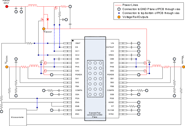 Figure 27. TPS4333x-Q1 Layout Example
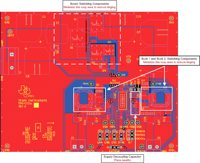 Figure 28. Layout Example (Top)
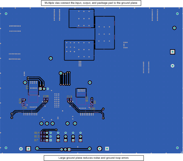 Figure 29. Layout Example (Bottom)
11.3 Power Dissipation Derating Profile, 38-Pin HTTSOP PowerPAD™ Package
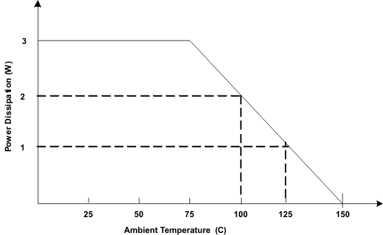 Figure 30. Derating Profile for Power Dissipation Based on High-K JEDEC PCB