SLVSA82F March 2011 – December 2014 TPS43330-Q1 , TPS43332-Q1
PRODUCTION DATA.
- 1 Features
- 2 Applications
- 3 Description
- 4 Revision History
- 5 Device Comparison Table
- 6 Pin Configuration and Functions
- 7 Specifications
-
8 Detailed Description
- 8.1 Overview
- 8.2 Functional Block Diagram
- 8.3 Feature Description
- 8.4 Device Functional Modes
-
9 Application and Implementation
- 9.1 Application Information
- 9.2
Typical Application
- 9.2.1 Design Requirements
- 9.2.2
Detailed Design Procedure
- 9.2.2.1 Boost Component Selection
- 9.2.2.2 Boost Maximum Input Current IIN_MAX
- 9.2.2.3 Boost Inductor Selection, L
- 9.2.2.4 Inductor Ripple Current, IRIPPLE
- 9.2.2.5 Peak Current in Low-Side FET, IPEAK
- 9.2.2.6 Right Half-Plane Zero RHP Frequency, fRHP
- 9.2.2.7 Output Capacitor, COUTx
- 9.2.2.8 Bandwidth of Boost Converter, fC
- 9.2.2.9 Output Ripple Voltage Due to Load Transients, ∆VOUTx
- 9.2.2.10 Selection of Components for Type II Compensation
- 9.2.2.11 Input Capacitor, CIN
- 9.2.2.12 Output Schottky Diode D1 Selection
- 9.2.2.13 Low-Side MOSFET (BOT_SW3)
- 9.2.2.14 BuckA Component Selection
- 9.2.2.15 Inductor Selection L
- 9.2.2.16 Inductor Ripple Current IRIPPLE
- 9.2.2.17 Output Capacitor COUTA
- 9.2.2.18 Bandwidth of Buck Converter fC
- 9.2.2.19 Selection of Components for Type II Compensation
- 9.2.2.20 Resistor Divider Selection for Setting VOUTA Voltage
- 9.2.2.21 BuckB Component Selection
- 9.2.2.22 Resistor Divider Selection for Setting VOUT Voltage
- 9.2.2.23 BuckX High-Side and Low-Side N-Channel MOSFETs
- 9.2.3 Application Curves
- 10Power Supply Recommendations
- 11Layout
- 12Device and Documentation Support
- 13Mechanical, Packaging, and Orderable Information
1 Features
- Qualified for Automotive Applications
- AEC-Q100 Qualified With the Following Results:
- Device Temperature Grade 1: –40°C to 125°C Ambient Operating Temperature
- Device HBM ESD Classification Level 2
- Device CDM ESD Classification Level C4B
- Two Synchronous Buck Controllers
- One Pre-Boost Controller
- Input Range up to 40 V, (Transients up to 60 V), Operation Down to 2 V When Boost is Enabled
- Low-Power-Mode IQ: 30 µA (One Buck On), 35 µA (Two Bucks On)
- Low Shutdown Current Ish < 4 µA
- Buck Output Range 0.9 V to 11 V
- Boost Output Selectable: 7 V, 10 V, or 11 V
- Programmable Frequency and External Synchronization Range 150 kHz to 600 kHz
- Separate Enable Inputs (ENA, ENB)
- Frequency Spread Spectrum (TPS43332)
- Selectable Forced Continuous Mode or Automatic Low-Power Mode at Light Loads
- Sense Resistor or Inductor DCR Sensing
- Out-of-Phase Switching Between Buck Channels
- Peak Gate-Drive Current 1.5 A
- Thermally Enhanced 38-Pin HTSSOP (DAP) PowerPAD™ Package
2 Applications
- Automotive Start-Stop, Infotainment, Navigation Instrument Cluster Systems
- Industrial and Automotive Multi-Rail DC Power Distribution Systems and Electronic Control Units
3 Description
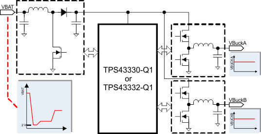
The TPS43330-Q1 and TPS43332-Q1 devices (TPS4333x-Q1) include two current-mode synchronous buck controllers and a voltage-mode boost controller. The TPS4333x-Q1 family of devices is ideally suited as a pre-regulator stage with low IQ requirements and for applications that must survive supply drops due to cranking events. The integrated boost controller allows the devices to operate down to 2 V at the input without seeing a drop on the buck regulator output stages. At light loads, the buck controllers can be enabled to operate automatically in low-power mode, consuming just 30 µA of quiescent current.
The buck controllers have independent soft-start capability and power-good indicators. Current foldback in the buck controllers and cycle-by-cycle current limitation in the boost controller provide external MOSFET protection. The switching frequency can be programed over 150 kHz to 600 kHz or synchronized to an external clock in the same range. Additionally, the TPS43332-Q1 device offers frequency-hopping spread-spectrum operation.
Device Information(1)
| PART NUMBER | PACKAGE | BODY SIZE (NOM) |
|---|---|---|
| TPS43330-Q1 | HTSSOP (38) | 12.50 mm × 6.20 mm |
| TPS43332-Q1 |
- For all available packages, see the orderable addendum at the end of the datasheet.
Typical Application Diagram
4 Revision History
Changes from E Revision (April 2013) to F Revision
- Added ESD Ratings table, Feature Description section, Device Functional Modes, Application and Implementation section, Power Supply Recommendations section, Layout section, Device and Documentation Support section, and Mechanical, Packaging, and Orderable Information sectionGo
Changes from D Revision (September 2012) to E Revision
- Revised descriptions for DIV, ENA, and ENB pinsGo
- Revised DC Electrical Characteristics, items 4.2, 4.4, and 4.6Go
- Replaced typical characteristic curve: LOAD STEP RESPONSE (BOOST) (0 TO 5 A AT 10 A/µs)Go
- Altered functional block diagramGo
- Revised last paragraph of Light-Load PFM Mode sectionGo
- Revised schematic for Application Example 1Go
- Changed R1 + R2... equation in Resistor Divider Selection... sectionGo
Changes from C Revision (July 2012) to D Revision
- Changed specification names for HBM and CDM classification ratingsGo
- Corrected TYP value for Vsense in Electrical Characteristics Go
- Corrected capacitor valueGo
Changes from B Revision (July 2012) to C Revision