ZHCSIV9F September   2009  – October 2018 TPS386000 , TPS386040

PRODUCTION DATA.  

  1. 特性
  2. 应用
  3. 说明
    1.     Device Images
      1.      TPS386000 典型应用电路: 监控 FPGA 的电源
  4. 修订历史记录
  5. Pin Configuration and Functions
    1.     Pin Functions
  6. Specifications
    1. 6.1 Absolute Maximum Ratings
    2. 6.2 ESD Ratings
    3. 6.3 Recommended Operating Conditions
    4. 6.4 Thermal Information
    5. 6.5 Electrical Characteristics
    6. 6.6 Timing Requirements
    7. 6.7 Switching Characteristics
    8. 6.8 Typical Characteristics
  7. Parameter Measurement Information
  8. Detailed Description
    1. 8.1 Overview
    2. 8.2 Functional Block Diagrams
    3. 8.3 Feature Description
      1. 8.3.1 Voltage Monitoring
      2. 8.3.2 Manual Reset
      3. 8.3.3 Watchdog Timer
      4. 8.3.4 Reset Output
    4. 8.4 Device Functional Modes
  9. Application and Implementation
    1. 9.1 Application Information
      1. 9.1.1 Undervoltage Detection
      2. 9.1.2 Undervoltage and Overvoltage Detection
      3. 9.1.3 Sensing a Negative Voltage
      4. 9.1.4 Reset Delay Time
    2. 9.2 Typical Application
      1. 9.2.1 Design Requirements
      2. 9.2.2 Detailed Design Procedure
      3. 9.2.3 Application Curves
  10. 10Power Supply Recommendations
  11. 11Layout
    1. 11.1 Layout Guidelines
    2. 11.2 Layout Example
  12. 12器件和文档支持
    1. 12.1 器件支持
      1. 12.1.1 开发支持
        1. 12.1.1.1 评估模块
        2. 12.1.1.2 Spice 模型
      2. 12.1.2 器件命名规则
    2. 12.2 文档支持
      1. 12.2.1 相关文档
    3. 12.3 相关链接
    4. 12.4 社区资源
    5. 12.5 商标
    6. 12.6 静电放电警告
    7. 12.7 术语表
  13. 13机械、封装和可订购信息

封装选项

机械数据 (封装 | 引脚)
散热焊盘机械数据 (封装 | 引脚)
订购信息

Switching Characteristics

Over the operating temperature range of TJ = –40°C to 125°C, 1.8 V < VDD < 6.5 V, RRESETn (n = 1, 2, 3, 4) = 100 kΩ to VDD (TPS386000 only), CRESETn (n = 1, 2, 3, 4L, 4H) = 50 pF to GND, RWDO = 100 kΩ to VDD, CWDO = 50 pF to GND, VMR = 100 kΩ to VDD, WDI = GND, and CTn (n = 1, 2, 3, 4) = open, unless otherwise noted. Typical values are at TJ = 25°C.
PARAMETER TEST CONDITIONS MIN TYP MAX UNIT
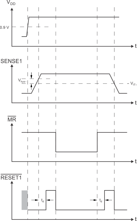
tD RESETn or RESETn delay time CTn = Open 14 20 24 ms
CTn = VDD 225 300 375
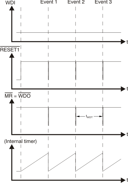
tWDT Watchdog timer time-out period(1) 450 600 750 ms
Start from RESET1 or RESET1 release or last WDI transition.
TPS386000 TPS386040 tim_svs-1_bvs105.gifFigure 1. SVS-1 Timing Diagram
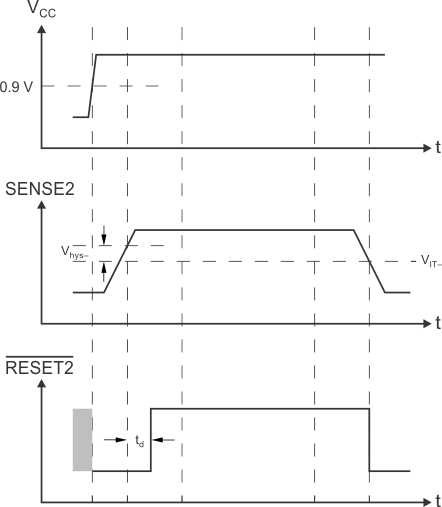
TPS386000 TPS386040 tim_svs-2_bvs105.gifFigure 2. SVS-2 Timing Diagram
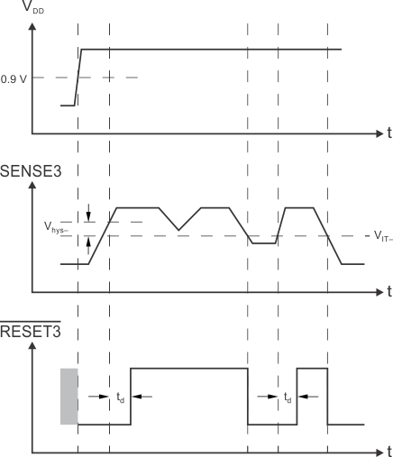
TPS386000 TPS386040 tim_svs-3_bvs105.gifFigure 3. SVS-3 Timing Diagram
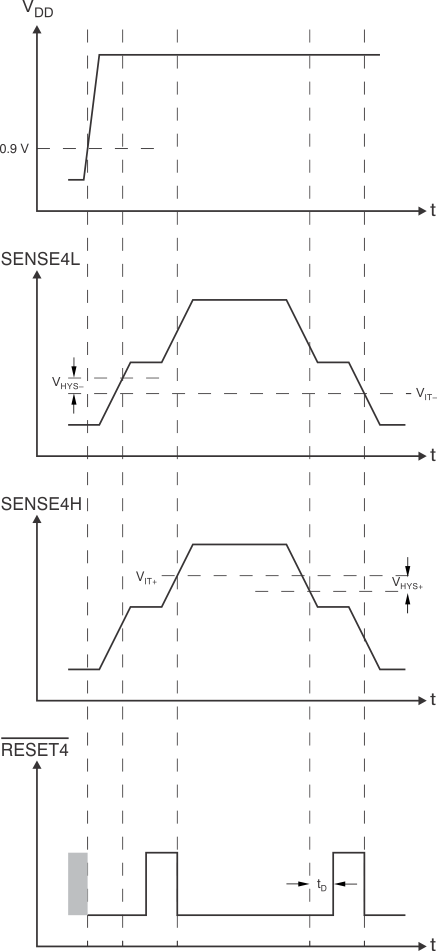
TPS386000 TPS386040 tim_svs-4_bvs105.gifFigure 4. SVS-4 Timing Diagram
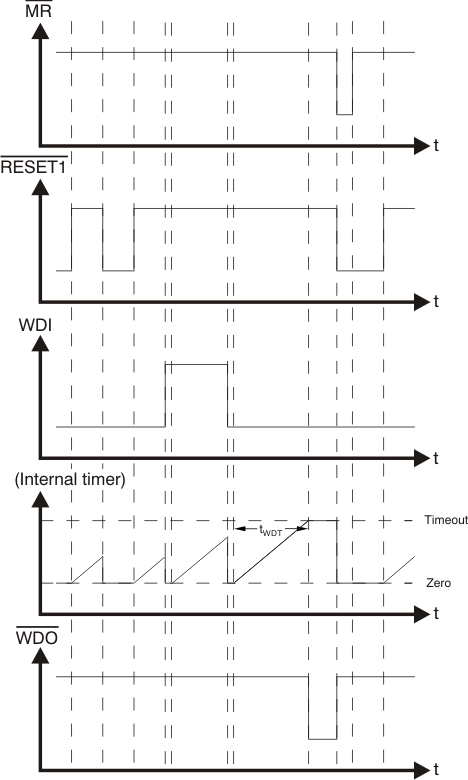
TPS386000 TPS386040 tim_wdt_bvs105.gifFigure 5. WDT Timing Diagram
TPS386000 TPS386040 tim_legacy_bvs105.gifFigure 6. Legacy WDT Configuration Timing Diagram
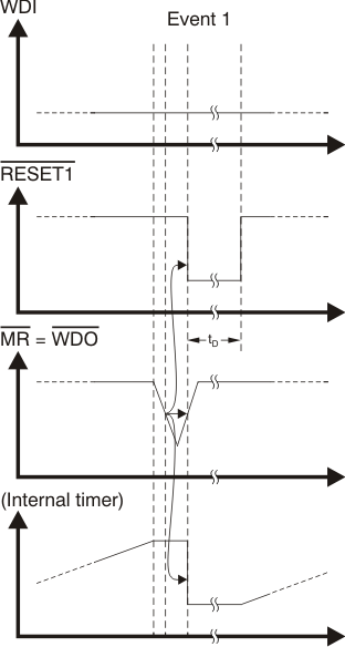
TPS386000 TPS386040 tim_legacy_enlargd_bvs105.gifFigure 7. Enlarged View of Event 1 from Figure 6