ZHCSKC4H May   2008  – October 2021

PRODMIX  

  1. 特性
  2. 应用
  3. 描述
  4. Revision History
  5. Pin Configuration and Functions
  6. Specifications
    1. 6.1 Absolute Maximum Ratings
    2. 6.2 ESD Ratings
    3. 6.3 Recommended Operating Conditions
    4. 6.4 Thermal Information
    5. 6.5 Electrical Characteristics
    6. 6.6 Timing Requirements
    7. 6.7 Switching Characteristics
    8. 6.8 Timing Diagrams
    9. 6.9 Typical Characteristics
  7. Detailed Description
    1. 7.1 Overview
    2. 7.2 Functional Block Diagram
    3. 7.3 Feature Description
      1. 7.3.1 Input Voltage (VDD)
        1. 7.3.1.1 VDD Hysteresis
        2. 7.3.1.2 VDD Glitch Immunity
      2. 7.3.2 Implemented Window-Watchdog Settings
        1. 7.3.2.1 Timing Rules of Window-Watchdog
      3. 7.3.3 Watchdog Software Considerations
    4. 7.4 Device Functional Modes
  8. Application and Implementation
    1. 8.1 Application Information
      1. 8.1.1 Lower-Boundary Calculation
    2. 8.2 Typical Application
      1. 8.2.1 Design Requirements
      2. 8.2.2 Detailed Design Procedure
        1. 8.2.2.1 Programming Window-Watchdog Using an External Capacitor
      3. 8.2.3 Application Curve
  9. Power Supply Recommendations
  10. 10Layout
    1. 10.1 Layout Guidelines
    2. 10.2 Layout Example
  11. 11Device and Documentation Support
    1. 11.1 Device Support
      1. 11.1.1 Device Nomenclature
    2. 11.2 Documentation Support
      1. 11.2.1 Related Documentation
    3. 11.3 接收文档更新通知
    4. 11.4 支持资源
    5. 11.5 Trademarks
    6. 11.6 Electrostatic Discharge Caution
    7. 11.7 术语表
  12. 12Mechanical, Packaging, and Orderable Information

封装选项

机械数据 (封装 | 引脚)
散热焊盘机械数据 (封装 | 引脚)
订购信息

Typical Characteristics

GUID-D0D73954-7FEA-4114-AADA-5D6FEE15AF56-low.gif
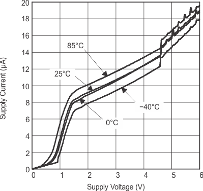
WDI = GNDWDT = GNDWDR = GND
  
Figure 6-2 Supply Current vs Supply Voltage
GUID-30F03736-4026-4A1B-B8EA-E6540E11898C-low.gif
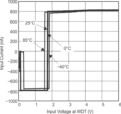
WDI = GNDWDR = GNDVDD = 6 V
Figure 6-4 Input Current vs Input Voltage at WDT
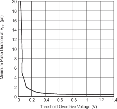
GUID-F40063C5-0900-4E82-99C5-245B0F32D8F9-low.gifFigure 6-6 Minimum Pulse Duration At VDD vs VDD Threshold Overdrive Voltage
GUID-421DA18F-9144-46FF-A43B-3E17254058DD-low.gif
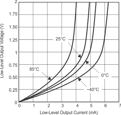
WDI = GNDWDT = GNDWDR = GND
VDD = 2 V
Figure 6-3 Low-Level Output Voltage vs Low-Level Output Current
GUID-52FE3EEB-3679-4C19-9646-E741EA2F2B8D-low.gif
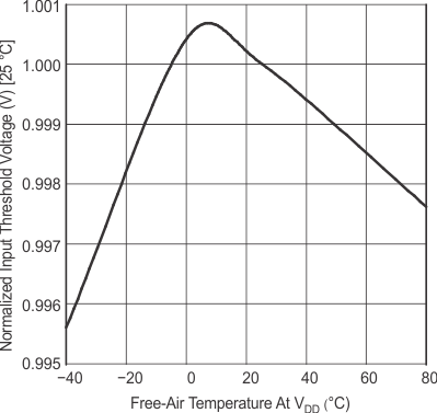
WDI = TriggeredWDT = GNDWDR = GND
Figure 6-5 Normalized Input Threshold Voltage vs Free-Air Temperature at VDD