ZHCSD07C November   2014  – February 2019 TPS3701

PRODUCTION DATA.  

  1. 特性
  2. 应用
  3. 说明
    1.     Device Images
      1.      典型应用
      2.      典型误差与结温之间的关系
  4. 修订历史记录
  5. Pin Configuration and Functions
    1.     Pin Functions
  6. Specifications
    1. 6.1 Absolute Maximum Ratings
    2. 6.2 ESD Ratings
    3. 6.3 Recommended Operating Conditions
    4. 6.4 Thermal Information
    5. 6.5 Electrical Characteristics
    6. 6.6 Timing Requirements
    7. 6.7 Typical Characteristics
  7. Detailed Description
    1. 7.1 Overview
    2. 7.2 Functional Block Diagram
    3. 7.3 Feature Description
      1. 7.3.1 Inputs (INA, INB)
      2. 7.3.2 Outputs (OUTA, OUTB)
    4. 7.4 Device Functional Modes
      1. 7.4.1 Normal Operation (VDD > UVLO)
      2. 7.4.2 Undervoltage Lockout (V(POR) < VDD < UVLO)
      3. 7.4.3 Power-On-Reset (VDD < V(POR))
  8. Application and Implementation
    1. 8.1 Application Information
      1. 8.1.1 Window Voltage Detector Considerations
      2. 8.1.2 Input and Output Configurations
      3. 8.1.3 Immunity to Input Pin Voltage Transients
    2. 8.2 Typical Application
      1. 8.2.1 Design Requirements
      2. 8.2.2 Detailed Design Procedure
      3. 8.2.3 Application Curve
  9. Power Supply Recommendations
  10. 10Layout
    1. 10.1 Layout Guidelines
    2. 10.2 Layout Example
  11. 11器件和文档支持
    1. 11.1 文档支持
      1. 11.1.1 相关文档
    2. 11.2 接收文档更新通知
    3. 11.3 社区资源
    4. 11.4 商标
    5. 11.5 静电放电警告
    6. 11.6 术语表
  12. 12机械、封装和可订购信息

封装选项

机械数据 (封装 | 引脚)
散热焊盘机械数据 (封装 | 引脚)
订购信息

Pin Configuration and Functions

DDC Package
6-Pin SOT
(Top View)
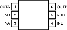
TPS3701 po_bvs240.gif

Pin Functions

PIN I/O DESCRIPTION
NAME NO.
GND 2 Ground
INA 3 I Comparator A input. This pin is connected to the voltage to be monitored with the use of an external resistor divider. When the voltage at this terminal drops below the threshold voltage VIT–(INA), OUTA is driven low.
INB 4 I Comparator B input. This pin is connected to the voltage to be monitored with the use of an external resistor divider. When the voltage at this terminal exceeds the threshold voltage VIT+(INB), OUTB is driven low.
OUTA 1 O INA comparator open-drain output. OUTA is driven low when the voltage at this comparator is less than VIT–(INA). The output goes high when the sense voltage rises above VIT+(INA).
OUTB 6 O INB comparator open-drain output. OUTB is driven low when the voltage at this comparator exceeds VIT+(INB). The output goes high when the sense voltage falls below VIT–(INB).
VDD 5 I Supply voltage input. Connect a 1.8-V to 36-V supply to VDD to power the device. It is good analog design practice to place a 0.1-µF ceramic capacitor close to this pin.