ZHCSHQ0B October   2017  – September 2019 TPS27S100

PRODUCTION DATA.  

  1. 1 特性
  2. 2 应用
  3. 3 说明
    1.     典型应用原理图
  4. 4 修订历史记录
  5. 5 Pin Configuration and Functions
    1.     Pin Functions
  6. 6 Specifications
    1. 6.1 Absolute Maximum Ratings
    2. 6.2 ESD Ratings
    3. 6.3 Recommended Operating Conditions
    4. 6.4 Thermal Information
    5. 6.5 Electrical Characteristics
    6. 6.6 Timing Requirements – Current Monitor Characteristics
    7. 6.7 Switching Characteristics
    8. 6.8 Typical Characteristics
  7. 7 Detailed Description
    1. 7.1 Overview
    2. 7.2 Functional Block Diagram
    3. 7.3 Feature Description
      1. 7.3.1 Accurate Current Monitor
      2. 7.3.2 Adjustable Current Limit
      3. 7.3.3 Inductive-Load Switching-Off Clamp
      4. 7.3.4 Full Protections and Diagnostics
        1. 7.3.4.1 Short-to-GND and Overload Detection
        2. 7.3.4.2 Open-Load Detection
        3. 7.3.4.3 Short-to-Supply Detection
        4. 7.3.4.4 Thermal Fault Detection
        5. 7.3.4.5 UVLO Protection
        6. 7.3.4.6 Loss of GND Protection
        7. 7.3.4.7 Reverse Current Protection
        8. 7.3.4.8 Protection for MCU I/Os
    4. 7.4 Device Functional Modes
      1. 7.4.1 Working Mode
  8. 8 Application and Implementation
    1. 8.1 Application Information
    2. 8.2 Typical Application
      1. 8.2.1 Design Requirements
      2. 8.2.2 Detailed Design Procedure
      3. 8.2.3 Application Curves
  9. 9 Power Supply Recommendations
  10. 10Layout
    1. 10.1 Layout Guidelines
    2. 10.2 Layout Example
      1. 10.2.1 Without a GND Network
      2. 10.2.2 With a GND Network
  11. 11器件和文档支持
    1. 11.1 接收文档更新通知
    2. 11.2 社区资源
    3. 11.3 商标
    4. 11.4 静电放电警告
    5. 11.5 Glossary
  12. 12机械、封装和可订购信息

封装选项

机械数据 (封装 | 引脚)
散热焊盘机械数据 (封装 | 引脚)
订购信息

With a GND Network

With a GND network, tie the thermal pad with a single trace through the GND network to the board GND copper.
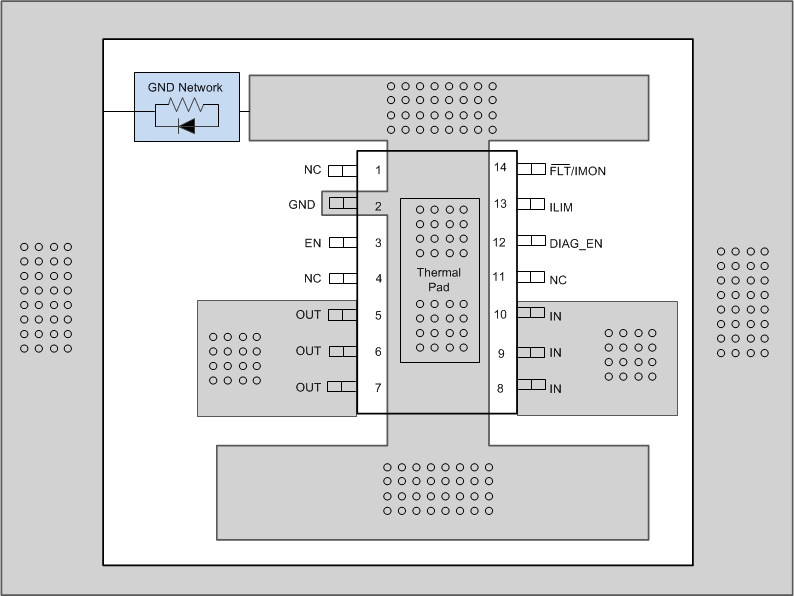
TPS27S100 Image21.gifFigure 39. Layout With a GND Network