ZHCSJV0G June 2018 – July 2021 TPS25830-Q1 , TPS25831-Q1
PRODUCTION DATA
- 1 特性
- 2 应用
- 3 说明
- 4 Revision History
- 5 说明(续)
- 6 Device Comparison Table
- 7 Pin Configuration and Functions
- 8 Specifications
- 9 Parameter Measurement Information
-
10Detailed Description
- 10.1 Overview
- 10.2 Functional Block Diagram
- 10.3
Feature Description
- 10.3.1 Buck Regulator
- 10.3.2 Enable/UVLO and Start-up
- 10.3.3 Switching Frequency and Synchronization (RT/SYNC)
- 10.3.4 Spread-Spectrum Operation
- 10.3.5 VCC, VCC_UVLO
- 10.3.6 Minimum ON-time, Minimum OFF-time
- 10.3.7 Internal Compensation
- 10.3.8 Bootstrap Voltage (BOOT)
- 10.3.9 RSNS, RSET, RILIMIT and RIMON
- 10.3.10 Overcurrent and Short Circuit Protection
- 10.3.11 Overvoltage, IEC and Short to Battery Protection
- 10.3.12 Cable Compensation
- 10.3.13 USB Port Control
- 10.3.14 FAULT Response
- 10.3.15 USB Specification Overview
- 10.3.16 USB Type-C® Basics
- 10.3.17 Device Power Pins (IN, CSN/OUT, and PGND)
- 10.3.18 Thermal Shutdown
- 10.3.19 Power Wake
- 10.3.20 Thermal Sensing with NTC (TPS25831-Q1)
- 10.4
Device Functional Modes
- 10.4.1 Shutdown Mode
- 10.4.2 Standby Mode
- 10.4.3 Active Mode
- 10.4.4 Device Truth Table (TT)
- 10.4.5 USB Port Operating Modes
- 10.4.6 High-Bandwidth Data-Line Switches (TPS25830-Q1 only)
-
11Application and Implementation
- 11.1 Application Information
- 11.2
Typical Application
- 11.2.1 Design Requirements
- 11.2.2
Detailed Design Procedure
- 11.2.2.1 Output Voltage
- 11.2.2.2 Switching Frequency
- 11.2.2.3 Inductor Selection
- 11.2.2.4 Output Capacitor Selection
- 11.2.2.5 Input Capacitor Selection
- 11.2.2.6 Bootstrap Capacitor Selection
- 11.2.2.7 VCC Capacitor Selection
- 11.2.2.8 Enable and Undervoltage Lockout Set-Point
- 11.2.2.9 Current Limit Set-Point
- 11.2.2.10 Cable Compensation Set-Point
- 11.2.2.11 LD_DET, POL, and FAULT Resistor Selection
- 11.2.3 Application Curves
- 12Power Supply Recommendations
- 13Layout
- 14Device and Documentation Support
- 15Mechanical, Packaging, and Orderable Information
10.3.16.4 Current Capability Advertisement and VCONN Overload Protection
The TPS2583x-Q1 supports all three Type-C current advertisements as defined by the USB Type-C standard. Current broadcast to a connected UFP is controlled by the CTRL1 and CTRL2 pins. For each broadcast level the device protects itself from a UFP that draws current in excess of the port’s USB Type-C Current advertisement by setting the current limit as shown in Table 10-8.
| DEVICE | CTRL1 | CTRL2 | CC CAPABILITY BROADCAST | MODE | SUPPORT USB 2.0 COMMUNICATION | CURRENT LIMIT (typ) |
|---|---|---|---|---|---|---|
| '830-Q1 | 0 | 0 | RESERVED, DO NOT USE | |||
| 0 | 1 | RESERVED, DO NOT USE | ||||
| 1 | 0 | 1.5 A | SDP | YES: DP_IN to DP_OUT and DM_IN to DM_OUT | BY RSNS, RSET, RILIMIT | |
| 1 | 1 | 3 A | CDP | YES: DP_IN to DP_OUT and DM_IN to DM_OUT | ||
| '831-Q1 | 0 | 0 | RESERVED, DO NOT USE | |||
| 0 | 1 | 3 A | DCP auto | NOT SUPPORT | BY RSNS, RSET, RILIMIT | |
| 1 | 0 | 1.5 A | SDP | Stub Connection Only | ||
| 1 | 1 | 3 A | CDP | Stub Connection Only | ||
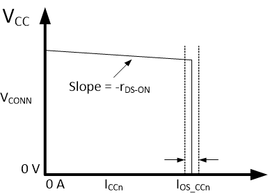
Under overload conditions, a precision current-limit circuit limits the VCONN output current. When a VCONN overload condition is present, the TPS2583x-Q1 maintains a constant output current, with the output voltage determined by (iOS_CCn x RLOAD). VCONN functionality is supported only with an external 5-V supply connected to VCC. Failure to connect an external supply may cause TPS2583x-Q1 Vcc reset. The device turns off when the junction temperature exceeds the thermal shutdown threshold, TSD and remains off until the junction temperature cools approximately 20°C and then restarts. The TPS2583x-Q1 current limit profile is shown in Figure 10-26.
 Figure 10-26 VCONN Current Limit Profile