ZHCSFH8D August   2016  – January 2018 TPS25741 , TPS25741A

UNLESS OTHERWISE NOTED, this document contains PRODUCTION DATA.  

  1. 特性
  2. 应用
  3. 说明
    1.     Device Images
      1.      DFP 主机端口中的简化实施方案
  4. 修订历史记录
  5. Device Comparison Table
  6. Pin Configuration and Functions
    1.     Pin Functions
  7. Specifications
    1. 7.1 Absolute Maximum Ratings
    2. 7.2 ESD Ratings
    3. 7.3 Recommended Operating Conditions
    4. 7.4 Thermal Information
    5. 7.5 Electrical Characteristics
    6. 7.6 Timing Requirements
    7. 7.7 Switching Characteristics
    8. 7.8 Typical Characteristics
  8. Detailed Description
    1. 8.1 Overview
      1. 8.1.1 VBUS Capacitance
      2. 8.1.2 USB Data Communications
    2. 8.2 Functional Block Diagram
    3. 8.3 Feature Description
      1. 8.3.1  USB Type-C CC Logic (CC1, CC2)
      2. 8.3.2  9.3.2 VCONN Supply (VCONN, CC1, CC2)
      3. 8.3.3  USB Power Delivery BMC Transmission (CC1, CC2, VTX)
      4. 8.3.4  USB Power Delivery BMC Reception (CC1, CC2)
      5. 8.3.5  Discharging (DSCG, VPWR)
        1. 8.3.5.1 Discharging after a Fault (VPWR)
      6. 8.3.6  Configuring Voltage Capabilities (HIPWR, EN9V, EN12V)
      7. 8.3.7  Configuring Power Capabilities (PSEL, PCTRL, HIPWR)
      8. 8.3.8  Gate Drivers
        1. 8.3.8.1 GDNG, GDNS
        2. 8.3.8.2 G5V
        3. 8.3.8.3 GDPG
      9. 8.3.9  Fault Monitoring and Protection
        1. 8.3.9.1 Over/Under Voltage (VBUS)
        2. 8.3.9.2 Over-Current Protection (ISNS, VBUS)
        3. 8.3.9.3 System Fault Input (GD, VPWR)
      10. 8.3.10 Voltage Control (CTL1, CTL2)
      11. 8.3.11 Sink Attachment Indicator (UFP, DVDD)
      12. 8.3.12 Accessory Attachment Indicator (AUDIO, DEBUG)
      13. 8.3.13 Plug Polarity Indication (POL)
      14. 8.3.14 Power Supplies (VAUX, VDD, VPWR, DVDD)
      15. 8.3.15 Grounds (AGND, GND)
      16. 8.3.16 Output Power Supply (DVDD)
    4. 8.4 Device Functional Modes
      1. 8.4.1 Sleep Mode
      2. 8.4.2 Checking VBUS at Start Up
  9. Application and Implementation
    1. 9.1 Application Information
      1. 9.1.1 System-Level ESD Protection
      2. 9.1.2 Use of GD Internal Clamp
      3. 9.1.3 Resistor Divider on GD for Programmable Start Up
      4. 9.1.4 Selection of the CTL1 and CTL2 Resistors (RFBL1 and RFBL2)
      5. 9.1.5 Voltage Transition Requirements
      6. 9.1.6 VBUS Slew Control using GDNG CSLEW
      7. 9.1.7 Tuning OCP Using RF and CF
    2. 9.2 Typical Applications
      1. 9.2.1 A/C Multiplexing Power Source
        1. 9.2.1.1 Design Requirements
        2. 9.2.1.2 Detailed Design Procedure
          1. 9.2.1.2.1 Power Pin Bypass Capacitors
          2. 9.2.1.2.2 Non-Configurable Components
          3. 9.2.1.2.3 Configurable Components
        3. 9.2.1.3 Application Curves
      2. 9.2.2 D/C Power Source
        1. 9.2.2.1 Design Requirements
        2. 9.2.2.2 Detailed Design Procedure
          1. 9.2.2.2.1 Power Pin Bypass Capacitors
          2. 9.2.2.2.2 Non-Configurable Components
          3. 9.2.2.2.3 Configurable Components
        3. 9.2.2.3 Application Curves
    3. 9.3 System Examples
      1. 9.3.1 A/C Power Source (Wall Adapter)
      2. 9.3.2 Dual-Port Power Managed A/C Power Source (Wall Adapter)
  10. 10Power Supply Recommendations
    1. 10.1 VDD
    2. 10.2 VCONN
    3. 10.3 VPWR
  11. 11Layout
    1. 11.1 Layout Guidelines
      1. 11.1.1 Port Current Kelvin Sensing
      2. 11.1.2 Power Pin Bypass Capacitors
      3. 11.1.3 Supporting Components
    2. 11.2 Layout Example
  12. 12器件和文档支持
    1. 12.1 Documentation Support
    2. 12.2 相关链接
    3. 12.3 Receiving Notification of Documentation Updates
    4. 12.4 Community Resources
    5. 12.5 商标
    6. 12.6 静电放电警告
    7. 12.7 Glossary
  13. 13机械、封装和可订购信息

封装选项

机械数据 (封装 | 引脚)
散热焊盘机械数据 (封装 | 引脚)
订购信息

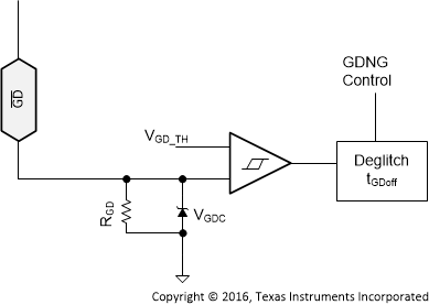
System Fault Input (GD, VPWR)

The gate-driver disable pin provides a method of overriding the internal control of GDNG and GDNS. A falling edge on GD disables the gate driver within tGDoff. If GD is held low after a sink is attached for 600 ms then a hard reset will be generated and the device sends a hard reset and goes through its startup process again.

The GD input can be controlled by a voltage or current source. An internal voltage clamp is provided to limit the input voltage in current source applications. The clamp can safely conduct up to 80 µA and will remain high impedance up to VGDC before clamping.
TPS25741 TPS25741A Overcurrent2_slvsdj5.gifFigure 39. Overcurrent Protection Circuit

If the VPWR pin remains below its falling UVLO threshold (VPWR_TH) for more than 600 ms after a sink is attached then the devices consider it a fault and will not enable GDNG. If the VPWR pin is between the rising and falling UVLO threshold, the TPS25741/TPS25741A may enable GDNG and proceed with normal operations. However, after GDNG is enabled, if the VBUS pin does not rise above its UVLO within 190 ms the devices consider it a fast-shutdown fault and disables GDNG. Therefore, in order to ensure USB Type-C compliance and normal operation, the VPWR pin must be above its rising UVLO threshold (VPWR_TH) within 275 ms of when UFP is pulled low and the VBUS pin must be above VBUS_RTH within 190 ms of GDNG being enabled.