ZHCSK65E November   2006  – October 2019 TPS2410 , TPS2411

PRODUCTION DATA.  

  1. 特性
  2. 应用
  3. 说明
    1.     Device Images
      1.      典型应用图
  4. 修订历史记录
  5. Device Comparison
  6. Pin Configuration and Functions
    1.     Pin Functions, PW
    2.     Pin Functions, RMS
  7. Specifications
    1. 7.1 Absolute Maximum Ratings
    2. 7.2 ESD Ratings
    3. 7.3 Recommended Operating Conditions
    4. 7.4 Thermal Information
    5. 7.5 Electrical Characteristics: TPS2410, 11
    6. 7.6 Typical Characteristics
  8. Detailed Description
    1. 8.1 Overview
    2. 8.2 Functional Block Diagram
    3. 8.3 Feature Description
      1. 8.3.1 Device Pins
        1. 8.3.1.1  A, C:
        2. 8.3.1.2  BYP:
        3. 8.3.1.3  FLTR:
        4. 8.3.1.4  FLTB:
        5. 8.3.1.5  GATE:
        6. 8.3.1.6  GND:
        7. 8.3.1.7  RSET:
        8. 8.3.1.8  RSVD:
        9. 8.3.1.9  STAT
        10. 8.3.1.10 UV, OV, PG:
        11. 8.3.1.11 VDD:
      2. 8.3.2 Gate Drive, Charge Pump and C(BYP)
      3. 8.3.3 Fast Comparator Input Filtering – C(FLTR)
      4. 8.3.4 UV, OV, and PG
      5. 8.3.5 Input ORing and Stat
    4. 8.4 Device Functional Modes
      1. 8.4.1 TPS2410 vs TPS2411 – MOSFET Control Methods
  9. Application and Implementation
    1. 9.1 Typical Connections
      1. 9.1.1 N+1 Power Supply
      2. 9.1.2 Input ORing
    2. 9.2 Typical Application Examples
      1. 9.2.1 VDD, BYP, and Powering Options
      2. 9.2.2 Bidirectional Blocking and Protection of C
      3. 9.2.3 ORing Examples
      4. 9.2.4 Design Requirements
        1. 9.2.4.1 MOSFET Selection and R(RSET)
        2. 9.2.4.2 TPS2410 Regulation-loop Stability
      5. 9.2.5 Detailed Design Procedure
      6. 9.2.6 Application Curves
  10. 10Power Supply Recommendations
    1. 10.1 Recommended Operating Range
    2. 10.2 System Design and Behavior with Transients
  11. 11Layout
    1. 11.1 Layout Considerations
    2. 11.2 Layout Example
  12. 12器件和文档支持
    1. 12.1 器件支持
    2. 12.2 相关链接
    3. 12.3 接收文档更新通知
    4. 12.4 社区资源
    5. 12.5 商标
    6. 12.6 静电放电警告
    7. 12.7 Glossary
  13. 13机械、封装和可订购信息

封装选项

机械数据 (封装 | 引脚)
散热焊盘机械数据 (封装 | 引脚)

Application Curves

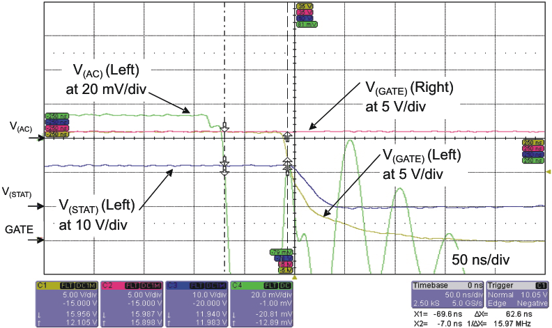
TPS2410 TPS2411 typ_off_12v_lvs727.gif
VDD = 12 I(LOAD) = 5 A
Figure 17. Typical Turnoff with Two Ored Devices Active vs IRL3713 Transient Applied to Left Side
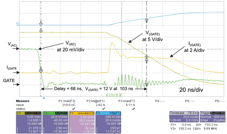
TPS2410 TPS2411 toff_10nf_12v_lvs727.gif
C(GATE) = 10 nF V(AC) = -20 mV
VDD = VA = 12 V
Figure 19. Turnoff Time
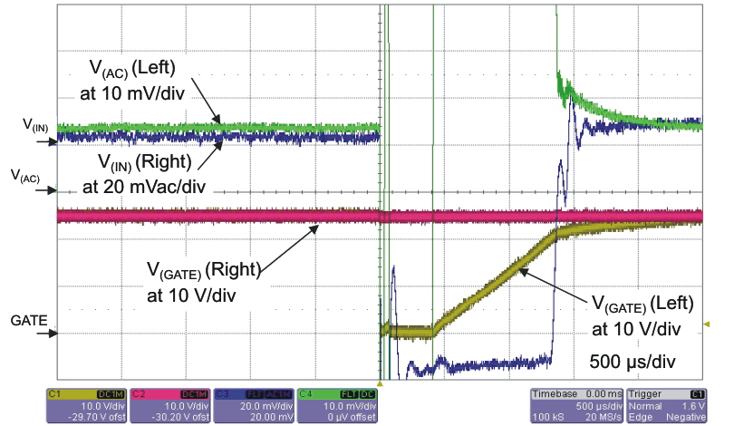
TPS2410 TPS2411 typ_off_3v_lvs727.gif
VDD = 3 V VA = 18 V I(LOAD) = 5 A
Figure 18. Typical Turnoff and Recovery with Two Ored Devices Active vs IRL3713 Transient Applied to Left Side
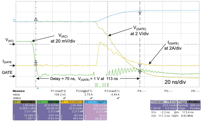
TPS2410 TPS2411 toff_10nf_1v_lvs727.gif
C(GATE) = 10 nF V(AC) = -20 mV VDD = 5
VA = 1 V
Figure 20. Turnoff Time