ZHCSK65E November 2006 – October 2019 TPS2410 , TPS2411
PRODUCTION DATA.
- 1 特性
- 2 应用
- 3 说明
- 4 修订历史记录
- 5 Device Comparison
- 6 Pin Configuration and Functions
- 7 Specifications
- 8 Detailed Description
- 9 Application and Implementation
- 10Power Supply Recommendations
- 11Layout
- 12器件和文档支持
- 13机械、封装和可订购信息
9.2.2 Bidirectional Blocking and Protection of C
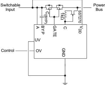
The TPS2410 and TPS2411 may be used in applications where bidirectional blocking is desired. This may occur in situations where two different voltages are ORed together, and operation from the lower voltage is desired. Another important application allows isolation of a redundant unit that is generating too high an output voltage. There are two considerations, first is the selection of the VDD source, and second is protection of the C pin from excessive current. Figure 13 provides an example of this type of application.
VDD needs to have voltage applied when A is to be connected to the load. Connecting VDD to C only works when voltage on C is always present before A is connected. VDD may be connected to A, a separate supply, or have voltage from A ORed with voltage from C. OV may be used to force GATE low, even when V(A) is greater than V(C), by driving OV to a voltage between 0.6 V and less than 5.25 V.
The C pin must be protected from excessive current if V(A) can exceed V(C) by more than 5.5 V. With a single MOSFET, V(C) is never more than a diode drop lower than V(A). When V(AC) is greater than a diode drop, a small current flows out of the C pin into the load. If V(AC) exceeds 5.5 V, a current limiting circuit should be used to protect C. Figure 13 provides an example circuit. Inserting this protection circuit creates a small offset in the forward regulation and threshold voltage.
 Figure 13. Bidirectional Blocking Example