ZHCSK65E November 2006 – October 2019 TPS2410 , TPS2411
PRODUCTION DATA.
- 1 特性
- 2 应用
- 3 说明
- 4 修订历史记录
- 5 Device Comparison
- 6 Pin Configuration and Functions
- 7 Specifications
- 8 Detailed Description
- 9 Application and Implementation
- 10Power Supply Recommendations
- 11Layout
- 12器件和文档支持
- 13机械、封装和可订购信息
9.2.5 Detailed Design Procedure
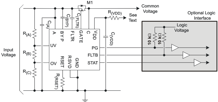
The following is a summarized design procedure:
- Choose between the TPS2410 or TPS2411, see TPS2410 vs TPS2411 – MOSFET Control Methods.
- Choose the VDD source. Table 2 provides a guide for where to connect VDD that covers most cases. VDD may be directly connected to the supply, but an R(VDD) / C(VDD) of 10 Ω / 0.01 μF is recommended.
- Noise voltage and impedance at the A pin should be kept low. C(A) may be required if there is noise on the bus, or A is not low impedance. If either of these is a concern, a C(A) of 0.01 μF or more may be required.
- Select C(BYP) as 2200 pF, X7R, 25-V or 50-V ceramic capacitor.
- If the noise and transient environment is not well known, design C(FLTR) in, then experimentally determine if it is required. Start with a 100 pF, X7R, 25-V or 50-V ceramic capacitor and adjust if necessary.
- Select M1 based on considerations of voltage drop, power dissipated, voltage ratings, and gate capacitance. See sections: MOSFET Selection and RSET and TPS2410 Regulation-Loop Stability.
- Select R(RSET) based on which MOSFET was chosen and reverse current considerations – see MOSFET Selection and RSET. If the noise and transient environment is not well known, make provision for R(RSET) even when using the TPS2410.
- Configure the UV and OV inputs per the desired behavior – UV, OV, and PG. Calculate the resistor dividers.
- Add optional interface for PG, FLTB, and STAT as desired.
- Make sure to connect RSVD to ground.
Table 2. VDD Connection Guide
| VA < 3 V | 3 V ≤ VA ≤ 3.5 V | VA > 3.5 V |
|---|---|---|
| Bias Supply > 3 V | VA or Bias Supply > 3 V. VC if always > 3 V | VC, VA or Bias for special configurations |
 Figure 16. Design Template