ZHCSDD9A November 2014 – February 2015 TPS22968-Q1
PRODUCTION DATA.
- 1 特性
- 2 应用
- 3 说明
- 4 修订历史记录
- 5 Pin Configuration and Functions
-
6 Specifications
- 6.1 Absolute Maximum Ratings
- 6.2 ESD Ratings
- 6.3 Recommended Operating Conditions
- 6.4 Thermal Information
- 6.5 Electrical Characteristics (VBIAS = 5 V)
- 6.6 Electrical Characteristics (VBIAS = 3.3 V)
- 6.7 Electrical Characteristics (VBIAS = 2.5 V)
- 6.8 Switching Characteristics
- 6.9 Typical DC Characteristics
- 6.10 Typical AC Characteristics
- 7 Parameter Measurement Information
- 8 Detailed Description
- 9 Application and Implementation
- 10Power Supply Recommendations
- 11Layout
- 12器件和文档支持
- 13机械封装和可订购信息
9 Application and Implementation
NOTE
Information in the following applications sections is not part of the TI component specification, and TI does not warrant its accuracy or completeness. TI’s customers are responsible for determining suitability of components for their purposes. Customers should validate and test their design implementation to confirm system functionality.
9.1 Application Information
This section highlights some of the design considerations for implementing this device in various applications. A PSPICE model for this device is also available on the product page for further aid.
9.1.1 Input Capacitor (Optional)
To limit the voltage drop on the input supply caused by transient inrush currents when the switch turns on into a discharged load capacitor, a capacitor must be placed between VIN and GND. A 1-µF ceramic capacitor, CIN, placed close to the pins, is usually sufficient. Higher values of CIN can be used to further reduce the voltage drop during high-current applications. When switching heavy loads, TI recommends to have an input capacitor about 10× higher than the output capacitor to avoid excessive voltage drop.
9.1.2 Output Capacitor (Optional)
Due to the integrated body diode in the NMOS switch, TI highly recommends a CIN greater than CL. A CL greater than CIN can cause the voltage on VOUT to exceed VIN when the system supply is removed. This could result in current flow through the body diode from VOUT to VIN. TI recommends a CIN to CL ratio of 10 to 1 for minimizing VIN dip caused by inrush currents during startup.
9.1.3 VIN and VBIAS Voltage Range
For optimal RON performance, make sure VIN ≤ VBIAS. The device is still functional if VIN > VBIAS, but it will exhibit RON greater than what is listed in the Electrical Characteristics (VBIAS = 5 V) and Electrical Characteristics (VBIAS = 2.5 V). See Figure 34 for an example of a typical device. Notice the increasing RON as VIN exceeds VBIAS voltage. Be sure to never exceed the maximum voltage rating for VIN and VBIAS.
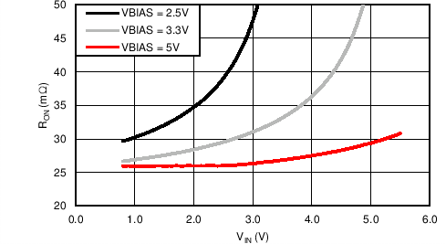
| TA = 25°C | IOUT = –200 mA |
9.1.3.1 Parallel Configuration
To increase the current capabilities and lower the RON by approximately 50%, both channels can be placed in parallel as shown in Figure 35 (parallel configuration). With this configuration, the CT1 and CT2 pins can be tied together to use one capacitor, CT, as shown in Figure 35. With a single CT capacitor, the rise time will be half of the typical rise-time value. Refer to the Table 1 for typical timing values.
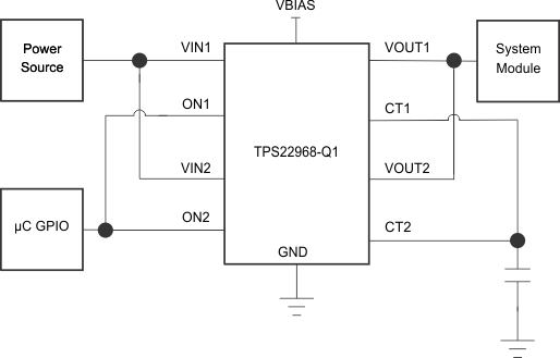 Figure 35. Parallel Configuration Schematic
9.1.3.2 Standby Power Reduction
TPS22968-Q1 can help to reduce the standby power consumption of a module. Some loads will consume a non-trivial amount of power when turned off. If the power to the load is removed by the load switch, the standby power consumption can be significantly reduced.
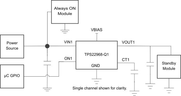 Figure 36. Standby Power Reduction Schematic
9.1.3.3 Power Supply Sequencing Without a GPIO Input
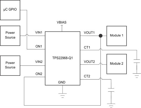
In many end equipments, there is a need to power up various modules in a predetermined manner. TPS22968-Q1 can solve the problem of power sequencing without adding any complexity to the overall system.
9.1.3.4 Reverse Current Blocking
In certain applications, it may be desirable to have reverse current blocking. Reverse current blocking prevents current from flowing from the output to the input of the load switch when the device is disabled. With the following configuration, the TPS22968-Q1 can be converted into a single-channel switch with reverse current blocking. In this configuration, VIN1 or VIN2 can be used as the input and VIN2 or VIN1 is the output.
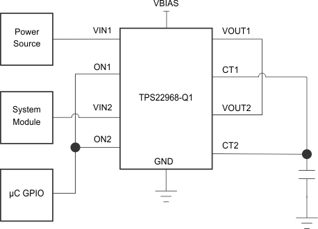 Figure 38. Reverse Current Blocking Schematic
9.2 Typical Application
This application demonstrates how the TPS22968-Q1 can be used to power a downstream load with a large capacitance. The example in Figure 39 is powering a 22-µF capacitive output load.
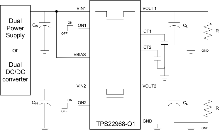 Figure 39. Typical Application Schematic for Powering a Downstream Module
9.2.1 Design Requirements
For this design example, use the following as the input parameters.
Table 3. Design Parameters
| DESIGN PARAMETER | EXAMPLE VALUE |
|---|---|
| VIN | 3.3 V |
| VBIAS | 5.0 V |
| Output capacitance (CL) | 22 µF |
| Allowable inrush current on VOUT | 0.400 A |
9.2.2 Detailed Design Procedure
To begin the design process, the designer needs to know the following:
- VIN voltage
- VBIAS voltage
- Output capacitance (CL)
- Allowable inrush current on VOUT due to CL capacitor
9.2.2.1 Inrush Current
To determine how much inrush current will be caused by the CL capacitor, use Equation 2.

where
- IINRUSH = amount of inrush current caused by CL
- CL = capacitance on VOUT
- dt = VOUT rise time
- dVOUT = increase in VOUT during the rise time
Inrush current is proportional to rise time. The rise time is adjustable by use of the CT capacitor. The appropriate rise time can be calculated using the design requirements and the inrush current equation (Equation 2).
To ensure an inrush current of less than 400 mA, choose a CT capacitor value that will yield a rise time of more than 182 µs. See the oscilloscope captures in the Application Curves for an example of how the CT capacitor can be used to reduce inrush current. See Table 1 for correlation between rise times and CT values.
An appropriate CL value should be placed on VOUT such that the IMAX and IPLS specifications of the device are not violated.
9.2.3 Application Curves
The two scope captures below show how the CT capacitor can be used to reduce inrush current.
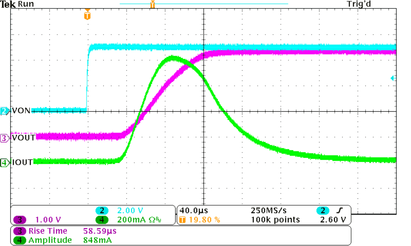
| VBIAS = 5 V | VIN = 3.3 V | TA = 25°C |
| CT = Open | CL = 22 µF |
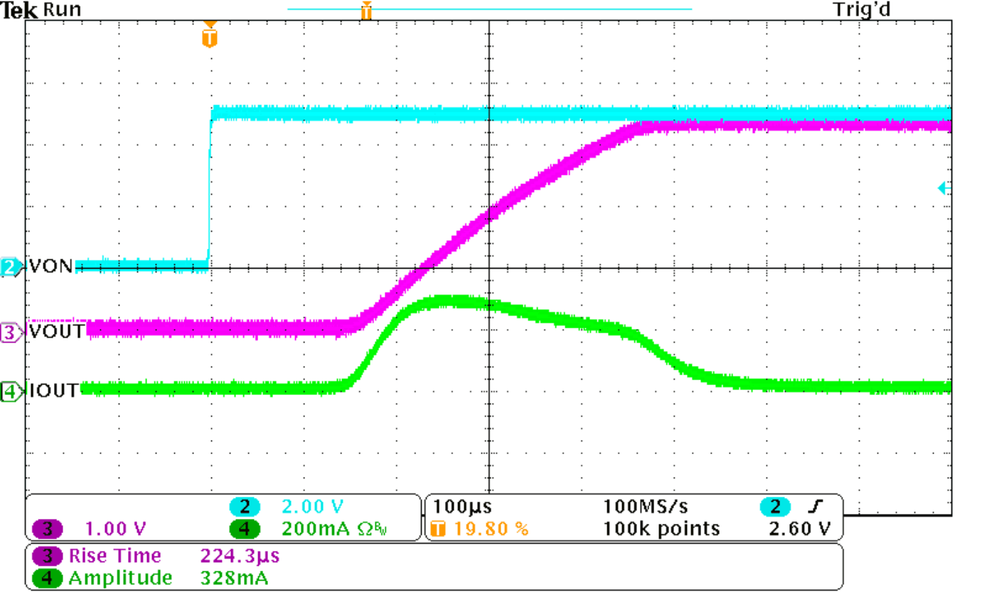
| VBIAS = 5 V | VIN = 3.3 V | TA = 25°C |
| CT = 220 pF | CL = 22 µF |