ZHCSA62B August 2012 – August 2014 TPS22965
PRODUCTION DATA.
9 Application and Implementation
9.1 Application Information
9.1.1 ON/OFF Control
The ON pin controls the state of the switch. Asserting ON high enables the switch. ON is active high and has a low threshold, making it capable of interfacing with low-voltage signals. The ON pin is compatible with standard GPIO logic thresholds. It can be used with any microcontroller with 1.2 V or higher GPIO voltage. This pin cannot be left floating and must be driven either high or low for proper functionality.
9.1.2 Input Capacitor (Optional)
To limit the voltage drop on the input supply caused by transient inrush currents when the switch turns on into a discharged load capacitor or short-circuit, a capacitor needs to be placed between VIN and GND. A 1-µF ceramic capacitor, CIN, placed close to the pins, is usually sufficient. Higher values of CIN can be used to further reduce the voltage drop during high current applications. When switching heavy loads, it is recommended to have an input capacitor about 10 times higher than the output capacitor to avoid excessive voltage drop.
9.1.3 Output Capacitor (Optional)
Due to the integrated body diode in the NMOS switch, a CIN greater than CL is highly recommended. A CL greater than CIN can cause VOUT to exceed VIN when the system supply is removed. This could result in current flow through the body diode from VOUT to VIN. A CIN to CL ratio of 10 to 1 is recommended for minimizing VIN dip caused by inrush currents during startup, however a 10 to 1 ratio for capacitance is not required for proper functionality of the device. A ratio smaller than 10 to 1 (such as 1 to 1) could cause slightly more VIN dip upon turn-on due to inrush currents. This can be mitigated by increasing the capacitance on the CT pin for a longer rise time (see Adjustable Rise Time section below).
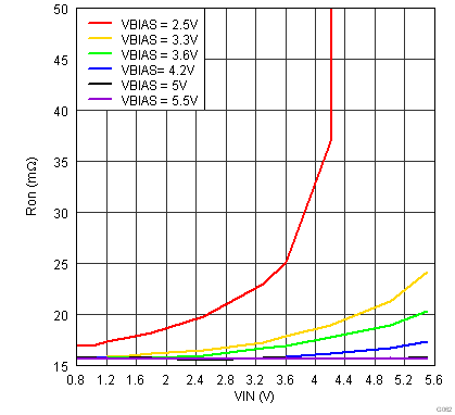
9.1.4 VIN and VBIAS Voltage Range
For optimal RON performance, make sure VIN ≤ VBIAS. The device will still be functional if VIN > VBIAS but it will exhibit RON greater than what is listed in the Electrical Characteristics table. See Figure 32 for an example of a typical device. Notice the increasing RON as VIN exceeds VBIAS voltage. Be sure to never exceed the maximum voltage rating for VIN and VBIAS.
| TA = 25 °C | IOUT = –200 mA |
9.2 Typical Application
This application demonstrates how the TPS22965 can be used to power downstream modules.
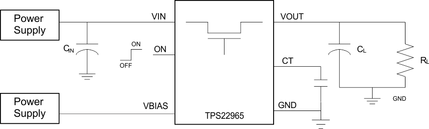 Figure 33. Powering a Downstream Module
9.2.1 Design Requirements
| DESIGN PARAMETER | EXAMPLE VALUE |
|---|---|
| VIN | 3.3 V |
| VBIAS | 5 V |
| CL | 22 µF |
| Maximum Acceptable Inrush Current | 400 mA |
9.2.2 Detailed Design Procedure
9.2.2.1 Inrush Current
When the switch is enabled, the output capacitors must be charged up from 0-V to the set value (3.3-V in this example). This charge arrives in the form of inrush current. Inrush current can be calculated using the following equation:
Where:
C = output capacitance
dV = output voltage
dt = rise time
The TPS22965 offers adjustable rise time for VOUT. This feature allows the user to control the inrush current during turn-on. The appropriate rise time can be calculated using the design requirements and the inrush current equation.
To ensure an inrush current of less than 400 mA, choose a CT value that will yield a rise time of more than 181.5 µs. See the oscilloscope captures below for an example of how the CT capacitor can be used to reduce inrush current.
9.2.3 Application Curves
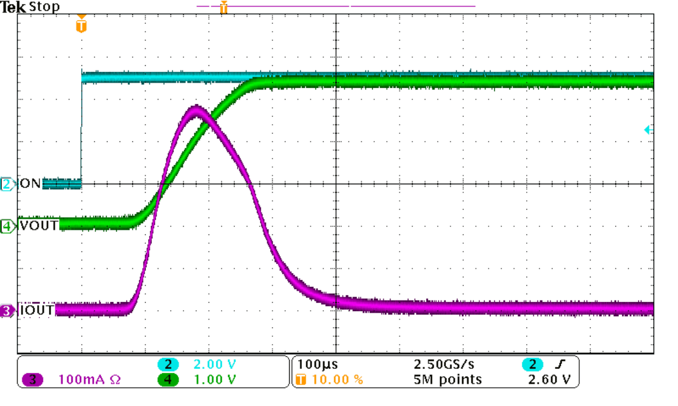
| VBIAS = 5 V | VIN = 3.3 V | CL = 22 µF |
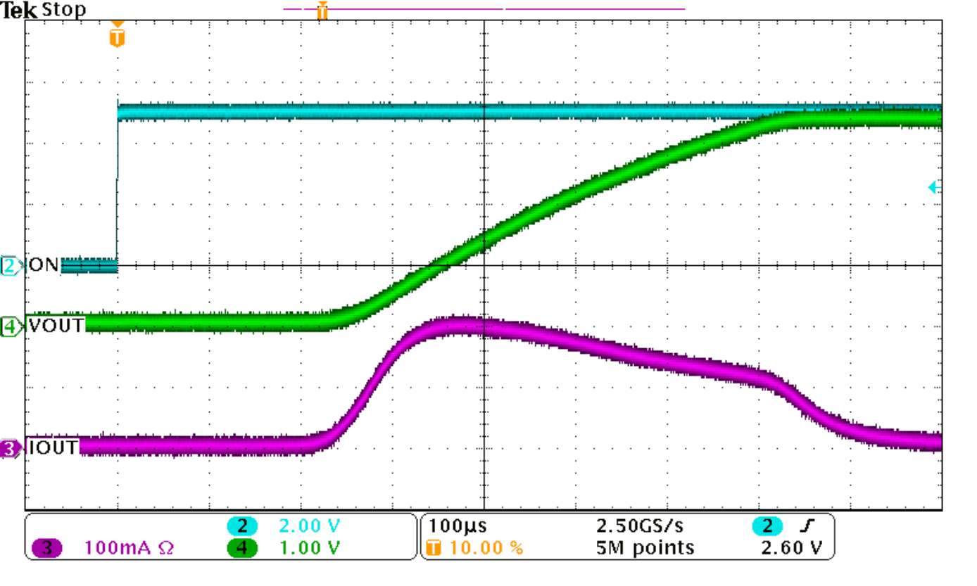
| VBIAS = 5 V | VIN = 3.3 V | CL = 22 µF |