ZHCSA62B August 2012 – August 2014 TPS22965
PRODUCTION DATA.
7 Specifications
7.1 Absolute Maximum Ratings
over operating free-air temperature range (unless otherwise noted)(1)(2)| MIN | MAX | UNIT | |||
|---|---|---|---|---|---|
| VIN | Input voltage range | –0.3 | 6 | V | |
| VOUT | Output voltage range | –0.3 | 6 | V | |
| VBIAS | Bias voltage range | –0.3 | 6 | V | |
| VON | Input voltage range | –0.3 | 6 | V | |
| IMAX | Maximum continuous switch current | 6 | A | ||
| IPLS | Maximum pulsed switch current, pulse <300 µs, 2% duty cycle | 8 | A | ||
| TJ | Maximum junction temperature | 125 | °C | ||
(1) Stresses beyond those listed under Absolute Maximum Ratings may cause permanent damage to the device. These are stress ratings only, and functional operation of the device at these or any other conditions beyond those indicated under Recommended Operating Conditions is not implied. Exposure to absolute–maximum–rated conditions for extended periods may affect device reliability.
(2) All voltage values are with respect to network ground terminal.
7.2 Handling Ratings
| MIN | MAX | UNIT | |||
|---|---|---|---|---|---|
| Tstg | Storage temperature range | –65 | 150 | °C | |
| V(ESD) | Electrostatic discharge | Human body model (HBM), per ANSI/ESDA/JEDEC JS-001, all pins(1) | –2000 | 2000 | V |
| Charged device model (CDM), per JEDEC specification JESD22-C101, all pins(2) | –1000 | 1000 | |||
(1) JEDEC document JEP155 states that 500-V HBM allows safe manufacturing with a standard ESD control process.
(2) JEDEC document JEP157 states that 250-V CDM allows safe manufacturing with a standard ESD control process.
7.3 Recommended Operating Conditions
| MIN | MAX | UNIT | |||
|---|---|---|---|---|---|
| VIN | Input voltage range | 0.8 | VBIAS | V | |
| VBIAS | Bias voltage range | 2.5 | 5.7 | V | |
| VON | ON voltage range | 0 | 5.7 | V | |
| VOUT | Output voltage range | VIN | V | ||
| VIH | High-level input voltage, ON | VBIAS = 2.5 V to 5.7 V | 1.2 | 5.7 | V |
| VIL | Low-level input voltage, ON | VBIAS = 2.5 V to 5.7 V | 0 | 0.5 | V |
| CIN | Input capacitor | 1(2) | µF | ||
| TA | Operating free-air temperature range(1) | –40 | 85 | °C | |
(1) In applications where high power dissipation and/or poor package thermal resistance is present, the maximum ambient temperature may have to be derated. Maximum ambient temperature [TA(max)] is dependent on the maximum operating junction temperature [TJ(max)], the maximum power dissipation of the device in the application [PD(max)], and the junction-to-ambient thermal resistance of the part/package in the application (θJA), as given by the following equation: TA(max) = TJ(max) – (θJA × PD(max))
(2) Refer to Application Information section.
7.4 Thermal Information
| THERMAL METRIC(1) | TPS22965 | UNIT | |
|---|---|---|---|
| DSG (8 PINS) | |||
| RθJA | Junction-to-ambient thermal resistance | 65.3 | °C/W |
| RθJC(top) | Junction-to-case (top) thermal resistance | 74.2 | |
| RθJB | Junction-to-board thermal resistance | 35.4 | |
| ψJT | Junction-to-top characterization parameter | 2.2 | |
| ψJB | Junction-to-board characterization parameter | 36.0 | |
| RθJC(bot) | Junction-to-case (bottom) thermal resistance | 12.8 | |
(1) For more information about traditional and new thermal metrics, see the IC Package Thermal Metrics application report, SPRA953.
7.5 Electrical Characteristics, VBIAS = 5.0 V
Unless otherwise noted, the specification in the following table applies over the operating ambient temperature –40 °C ≤ TA ≤ 85 °C (Full) and VBIAS = 5.0 V. Typical values are for TA = 25 °C.| PARAMETER | TEST CONDITIONS | TA | MIN | TYP | MAX | UNIT | ||
|---|---|---|---|---|---|---|---|---|
| POWER SUPPLIES AND CURRENTS | ||||||||
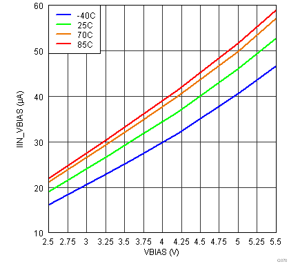
| IIN(VBIAS-ON) | VBIAS quiescent current | IOUT = 0 mA, VIN = VON = VBIAS = 5.0 V |
Full | 50 | 75 | µA | ||
| IIN(VBIAS-OFF) | VBIAS shutdown current | VON = GND, VOUT = 0 V | Full | 2 | µA | |||
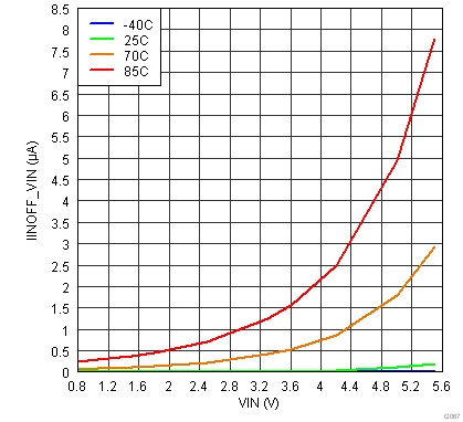
| IIN(VIN-OFF) | VIN off-state supply current | VON = GND, VOUT = 0 V |
VIN = 5.0 V | Full | 0.2 | 8 | µA | |
| VIN = 3.3 V | 0.02 | 3 | ||||||
| VIN = 1.8 V | 0.01 | 2 | ||||||
| VIN = 0.8 V | 0.005 | 1 | ||||||
| ION | ON pin input leakage current | VON = 5.5 V | Full | 0.5 | µA | |||
| RESISTANCE CHARACTERISTICS | ||||||||
| RON | ON-state resistance | IOUT = –200 mA, VBIAS = 5.0 V |
VIN = 5.0 V | 25°C | 16 | 23 | mΩ | |
| Full | 25 | |||||||
| VIN = 3.3 V | 25°C | 16 | 23 | mΩ | ||||
| Full | 25 | |||||||
| VIN = 1.8 V | 25°C | 16 | 23 | mΩ | ||||
| Full | 25 | |||||||
| VIN = 1.5 V | 25°C | 16 | 23 | mΩ | ||||
| Full | 25 | |||||||
| VIN = 1.2 V | 25°C | 16 | 23 | mΩ | ||||
| Full | 25 | |||||||
| VIN = 0.8 V | 25°C | 16 | 23 | mΩ | ||||
| Full | 25 | |||||||
| RPD | Output pull-down resistance | VIN = 5.0 V, VON = 0 V, IOUT = 15 mA | Full | 225 | 300 | Ω | ||
7.6 Electrical Characteristics, VBIAS = 2.5 V
Unless otherwise noted, the specification in the following table applies over the operating ambient temperature –40 °C ≤ TA ≤ 85 °C (Full) and VBIAS = 2.5 V. Typical values are for TA = 25 °C.| PARAMETER | TEST CONDITIONS | TA | MIN | TYP | MAX | UNIT | ||
|---|---|---|---|---|---|---|---|---|
| POWER SUPPLIES AND CURRENTS | ||||||||
| IIN(VBIAS-ON) | VBIAS quiescent current | IOUT = 0 mA, VIN = VON = VBIAS = 2.5 V |
Full | 20 | 30 | µA | ||
| IIN(VBIAS-OFF) | VBIAS shutdown current | VON = GND, VOUT = 0 V | Full | 2 | µA | |||
| IIN(VIN-OFF) | VIN off-state supply current | VON = GND, VOUT = 0 V |
VIN = 2.5 V | Full | 0.01 | 3 | µA | |
| VIN = 1.8 V | 0.01 | 2 | ||||||
| VIN = 1.2 V | 0.005 | 2 | ||||||
| VIN = 0.8 V | 0.003 | 1 | ||||||
| ION | ON pin input leakage current | VON = 5.5 V | Full | 0.5 | µA | |||
| RESISTANCE CHARACTERISTICS | ||||||||
| RON | ON-state resistance | IOUT = –200 mA, VBIAS = 2.5 V |
VIN = 2.5 V | 25°C | 20 | 26 | mΩ | |
| Full | 28 | |||||||
| VIN = 1.8 V | 25°C | 19 | 26 | mΩ | ||||
| Full | 28 | |||||||
| VIN = 1.5 V | 25°C | 18 | 25 | mΩ | ||||
| Full | 27 | |||||||
| VIN = 1.2 V | 25°C | 18 | 25 | mΩ | ||||
| Full | 27 | |||||||
| VIN = 0.8 V | 25°C | 17 | 25 | mΩ | ||||
| Full | 27 | |||||||
| RPD | Output pull-down resistance | VIN = 2.5 V, VON = 0 V, IOUT = 1 mA | Full | 275 | 325 | Ω | ||
7.7 Switching Characteristics
| PARAMETER | TEST CONDITION | MIN | TYP | MAX | UNIT | |
|---|---|---|---|---|---|---|
| VIN = VON = VBIAS = 5 V, TA = 25ºC (unless otherwise noted) | ||||||
| tON | Turn-on time | RL = 10 Ω, CL = 0.1 µF, CT = 1000 pF | 1325 | µs | ||
| tOFF | Turn-off time | 10 | ||||
| tR | VOUT rise time | 1625 | ||||
| tF | VOUT fall time | 3.5 | ||||
| tD | ON delay time | 500 | ||||
| VIN = 0.8 V, VON = VBIAS = 5 V, TA = 25ºC (unless otherwise noted) | ||||||
| tON | Turn-on time | RL = 10 Ω, CL = 0.1 µF, CT = 1000 pF | 600 | µs | ||
| tOFF | Turn-off time | 80 | ||||
| tR | VOUT rise time | 300 | ||||
| tF | VOUT fall time | 5.5 | ||||
| tD | ON delay time | 460 | ||||
| VIN = 2.5V, VON = 5 V, VBIAS = 2.5 V, TA = 25ºC (unless otherwise noted) | ||||||
| tON | Turn-on time | RL = 10 Ω, CL = 0.1 µF, CT = 1000 pF | 2200 | µs | ||
| tOFF | Turn-off time | 9 | ||||
| tR | VOUT rise time | 2275 | ||||
| tF | VOUT fall time | 3.1 | ||||
| tD | ON delay time | 1075 | ||||
| VIN = 0.8 V, VON = 5 V, VBIAS = 2.5 V, TA = 25ºC (unless otherwise noted) | ||||||
| tON | Turn-on time | RL = 10 Ω, CL = 0.1 µF, CT = 1000 pF | 1450 | µs | ||
| tOFF | Turn-off time | 60 | ||||
| tR | VOUT rise time | 875 | ||||
| tF | VOUT fall time | 5.5 | ||||
| tD | ON delay time | 1010 | ||||
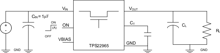
A. Rise and fall times of the control signal is 100 ns.
Figure 1. Test Circuit
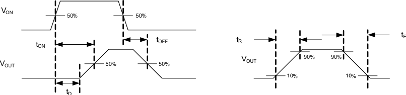 Figure 2. tON/tOFF Waveforms
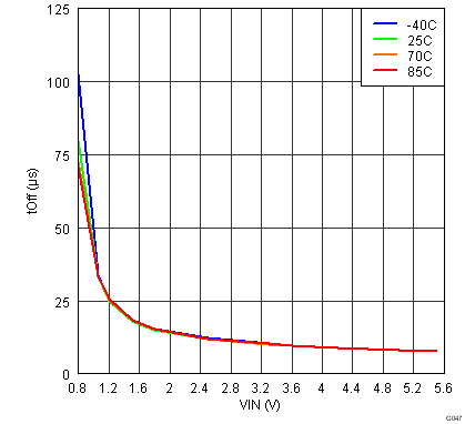
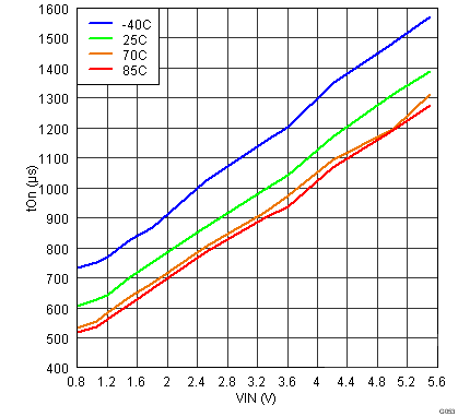
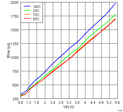
7.8 Typical Characteristics
| VIN = VBIAS | VON = 5 V | VOUT = Open |
| VBIAS = 5.5 V | VON = 0 V | VOUT = 0 V |
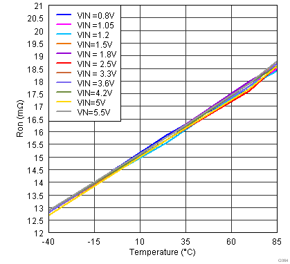
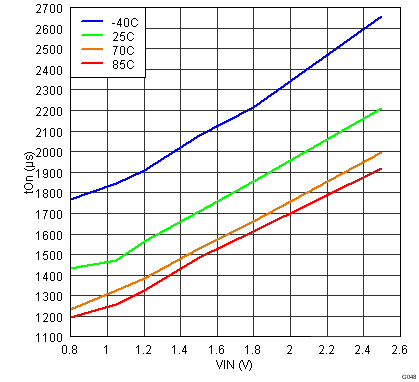
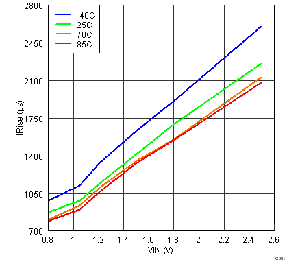
| VBIAS = 5.5 V | IOUT = –200 mA |
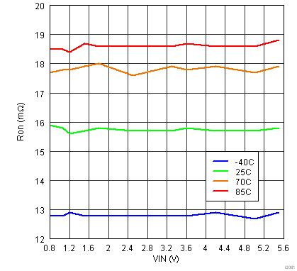
| VBIAS = 5.5 V | IOUT = –200 mA |
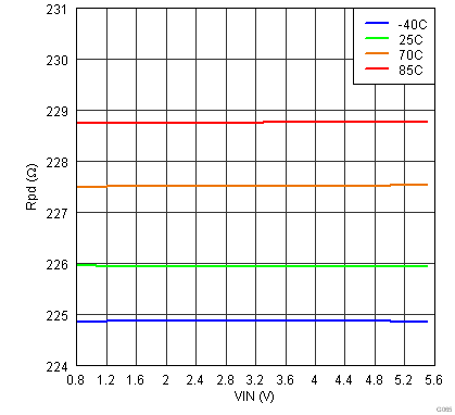
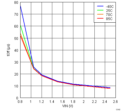
| VBIAS = 5.5 V | VON = 0 V | IPD = 1 mA |
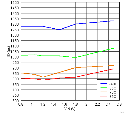
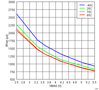
| VBIAS = 2.5 V | CT = 1 nF |
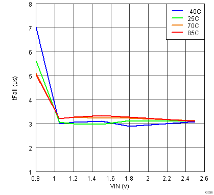
| VBIAS = 2.5 V | CT = 1 nF |
| VBIAS = 2.5 V | CT = 1 nF |
| VBIAS = 2.5 V | CT = 1 nF |
| VBIAS = 2.5 V | CT = 1 nF |
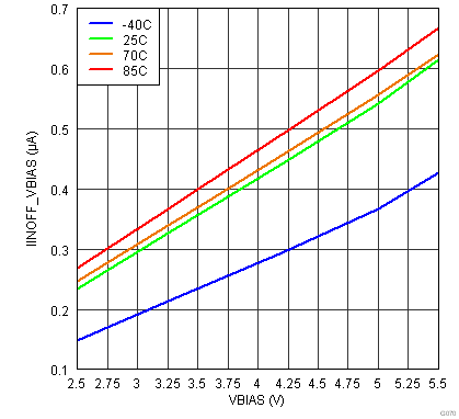
| VIN = 2.5 V | CT = 1 nF |
| VIN = VBIAS | VON = 0 V | VOUT = 0 V |
| VBIAS = 2.5 V | IOUT = –200 mA |
| VBIAS = 2.5 V | IOUT = –200 mA |
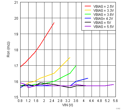
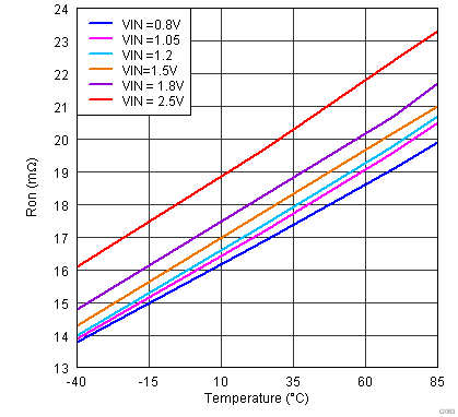
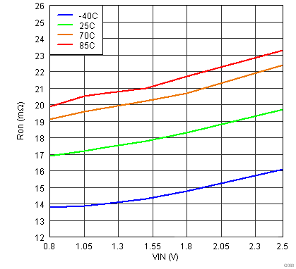
| TA = 25 °C | IOUT = –200 mA |
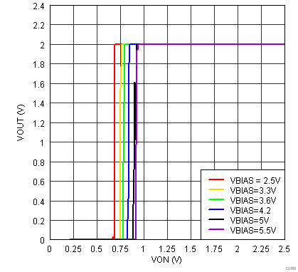
| TA = 25 °C | VIN = 2 V |
| VBIAS = 5.5 V | CT = 1 nF |
| VBIAS = 5.5 V | CT = 1 nF |
| VBIAS = 5.5 V | CT = 1 nF |
| VBIAS = 5.5 V | CT = 1 nF |
| VBIAS = 5.5 V | CT = 1 nF |
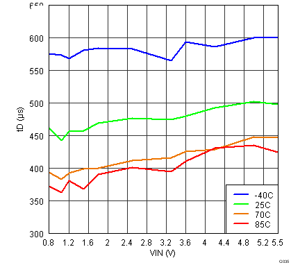
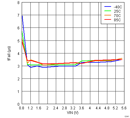
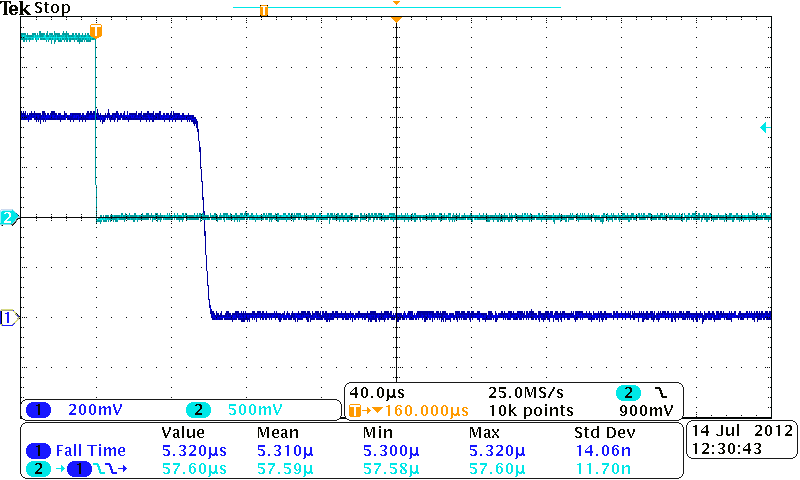
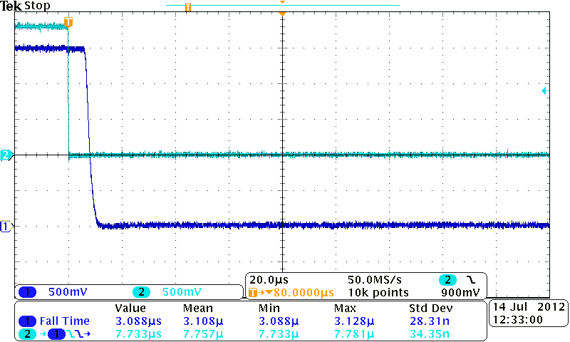
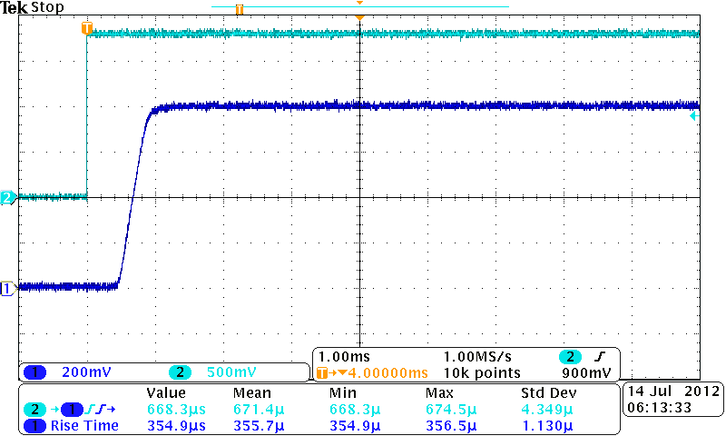
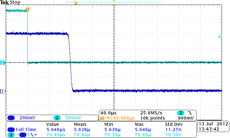
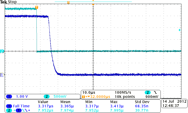
7.9 Typical Switching Characteristics
TA = 25 °C, CT = 1 nF, CIN = 1 µF, CL = 0.1 µF, RL = 10 Ω, CH1 = VOUT, CH2 = VON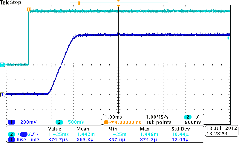
| VIN = 0.8 V | VBIAS = 2.5 V | CIN = 1 µF |
| CL = 0.1 µF | RL = 10 Ω |
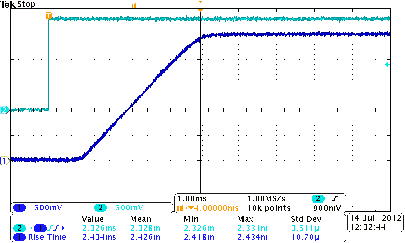
| VIN = 2.5 V | VBIAS = 2.5 V | CIN = 1 µF, |
| CL = 0.1 µF | RL = 10 Ω |
| VIN = 0.8 V | VBIAS = 2.5 V | CIN = 1 µF |
| CL = 0.1 µF | RL = 10 Ω |
| VIN = 2.5 V | VBIAS = 2.5 V | CIN = 1 µF |
| CL = 0.1 µF | RL = 10 Ω |
| VIN = 0.8 V | VBIAS = 5.0 V | CIN = 1 µF |
| CL = 0.1 µF | RL = 10 Ω |
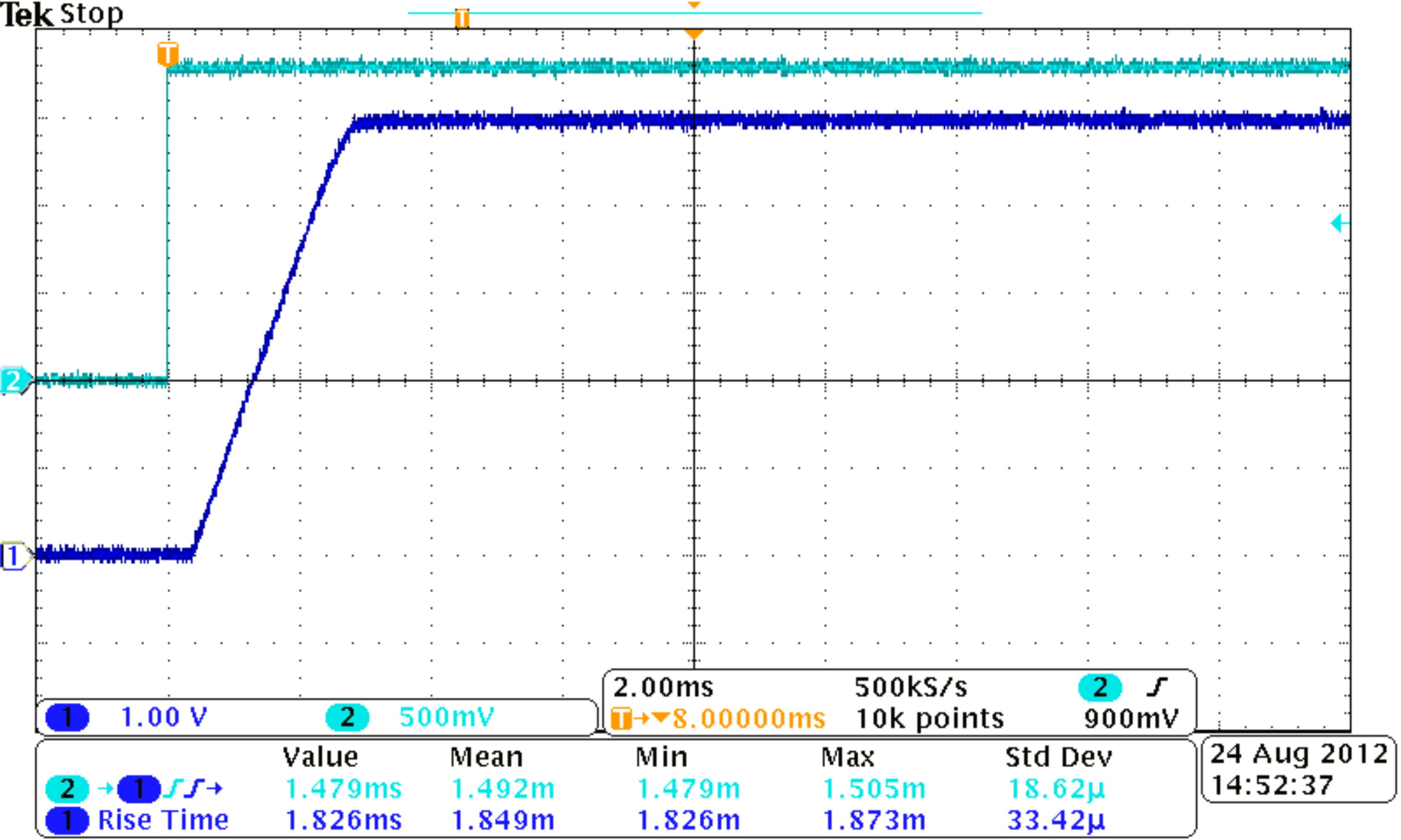
| VIN = 5.0 V | VBIAS = 5.0 V | CIN = 1 µF |
| CL = 0.1 µF | RL = 10 Ω |
| VIN = 0.8 V | VBIAS = 5.0 V | CIN = 1 µF |
| CL = 0.1 µF | RL = 10 Ω |
| VIN = 5.0 V | VBIAS = 5.0 V | CIN = 1 µF |
| CL = 0.1 µF | RL = 10 Ω) |