ZHCSA62B August 2012 – August 2014 TPS22965
PRODUCTION DATA.
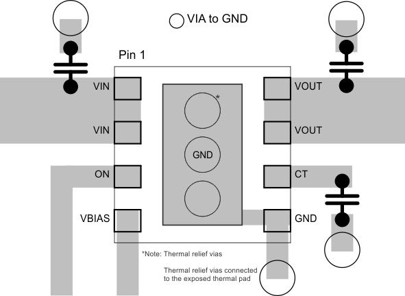
11 Layout
11.1 Layout Guidelines
For best performance, all traces should be as short as possible. To be most effective, the input and output capacitors should be placed close to the device to minimize the effects that parasitic trace inductances may have on normal operation. Using wide traces for VIN, VOUT, and GND helps minimize the parasitic electrical effects along with minimizing the case to ambient thermal impedance. The CT trace should be as short as possible to avoid parasitic capacitance.
11.2 Layout Example
11.3 Thermal Considerations
The maximum IC junction temperature should be restricted to 125°C under normal operating conditions. To calculate the maximum allowable dissipation, PD(max) for a given output current and ambient temperature, use the following equation as a guideline:
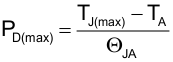
Where:
PD(max) = maximum allowable power dissipation
TJ(max) = maximum allowable junction temperature (125°C for the TPS22965)
TA = ambient temperature of the device
ΘJA = junction to air thermal impedance. See Thermal Information section. This parameter is highly dependent upon board layout.
Refer to the Layout Example, notice that the thermal vias are located under the exposed thermal pad of the device. This allows for thermal diffusion away from the device.