ZHCSAH4D November 2012 – July 2021
PRODUCTION DATA
- 1 特性
- 2 应用
- 3 说明
- 4 Revision History
- 5 Specifications
- 6 Pin Configuration and Functions
- 7 Parameter Measurement Information
- 8 Detailed Description
- 9 Application and Implementation
- 10Power Supply Recommendations
- 11Layout
- 12Device and Documentation Support
- 13Mechanical, Packaging, and Orderable Information
5.7.1 Typical AC Scope Captures at TA = 25°C
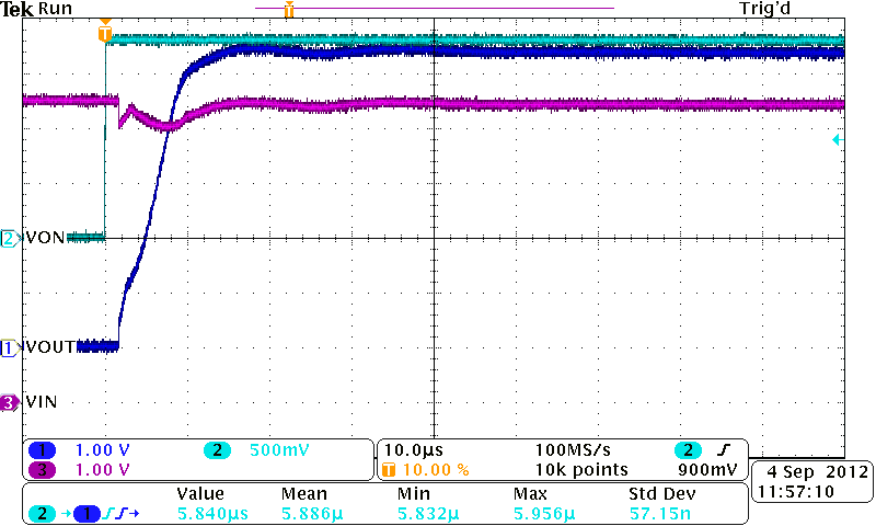 Figure 5-18 Turn-On Response Time (VIN = 5.5 V, CIN = 10 µF, CL = 1 µF, RL = 10 Ω)
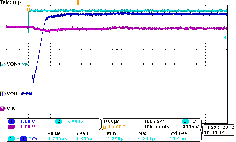 Figure 5-20 Turn-On Response Time (VIN = 5.5 V, CIN = 10 µF, CL = 0.1 µF, RL = 10 Ω)
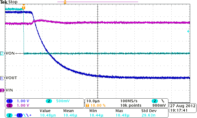 Figure 5-22 Turn-Off Response Time (VIN = 5.5 V, CIN = 10 µF, CL = 1 µF, RL = 10 Ω)
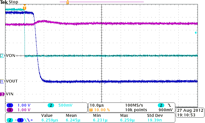 Figure 5-24 Turn-Off Response Time (VIN = 5.5 V, CIN = 10 µF, CL = 0.1 µF, RL = 10 Ω)
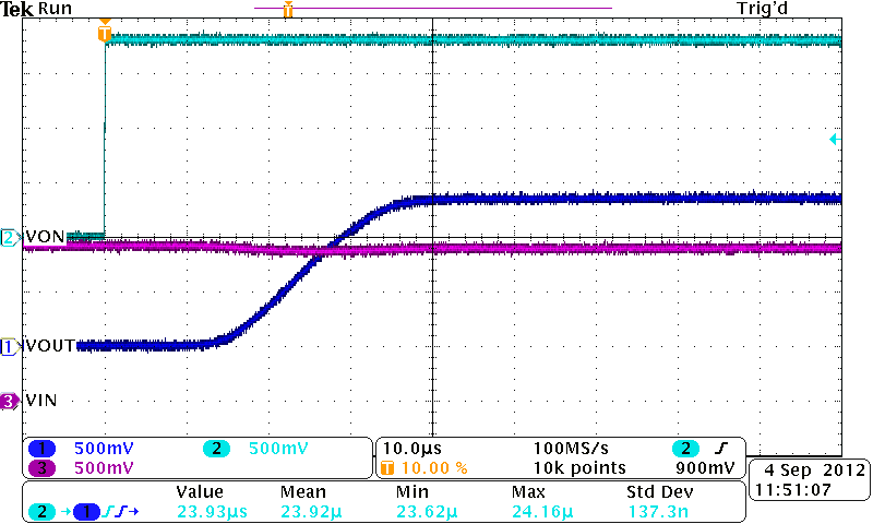 Figure 5-19 Turn-On Response Time (VIN = 1.4 V, CIN = 10 µF, CL = 1 µF, RL = 10 Ω)
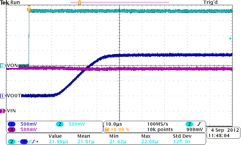 Figure 5-21 Turn-On Response Time (VIN = 1.4 V, CIN = 10 µF, CL = 0.1 µF, RL = 10 Ω)
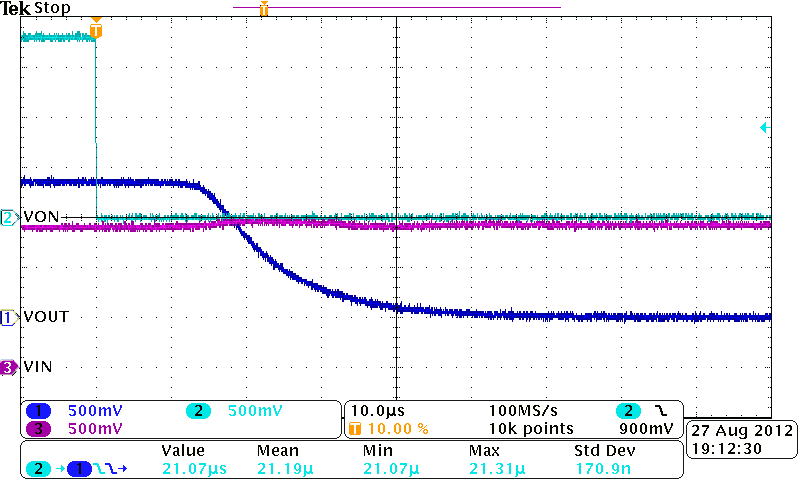 Figure 5-23 Turn-Off Response Time (VIN = 1.4 V, CIN = 10 µF, CL = 1 µF, RL = 10 Ω)
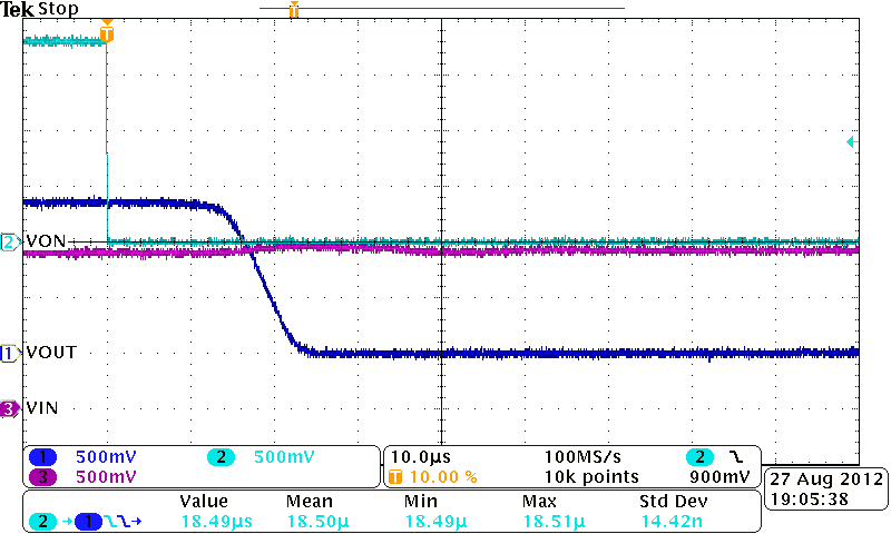 Figure 5-25 Turn-Off Response Time (VIN = 1.4 V, CIN = 10 µF, CL = 0.1 µF, RL = 10 Ω)