ZHCSEX7C November 2015 – February 2016 TPS22925
PRODUCTION DATA.
8 Detailed Description
8.1 Overview
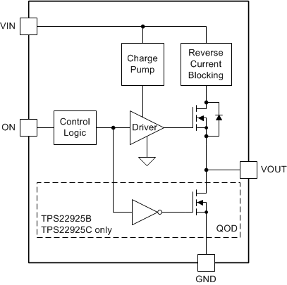
The TPS22925 is a single channel, 3-A load switch in a WCSP-6 package. This device implements an N-channel MOSFET with a controlled rise time for applications that need to limit inrush current. The device is also designed to have low leakage current during off state. This prevents downstream circuits from pulling high standby current from the supply. The TPS22925 provides reverse current blocking when the power switch is disabled. Integrated control logic, driver, and output discharge FET eliminates the need for additional external components, which reduces solution size and bill of material (BOM) count.
8.2 Functional Block Diagram

8.3 Feature Description
8.3.1 ON and OFF Control
The ON pin controls the state of the switch. Asserting the ON pin high enables the switch. The ON pin is compatible with GPIOs of 1.5 V and above.
8.3.2 Quick Output Discharge (QOD) (TPS22925B and TPS22925C only)
When the switch is disabled, a discharge path is enabled between the output and ground with a typical resistance of 150 Ω. The resistance pulls down the output and prevents it from floating when the device is disabled.
8.3.3 Reverse Current Blocking
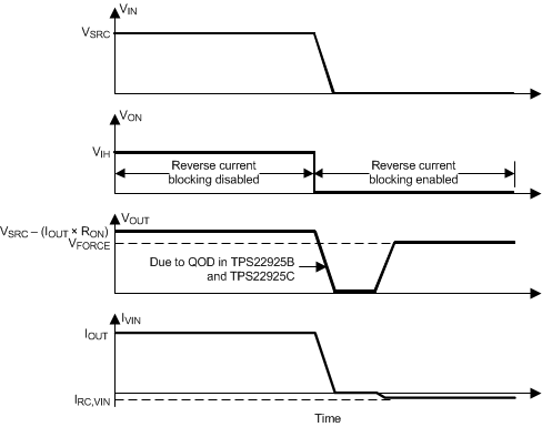
The reverse current blocking feature prevents current flow from the VOUT pin to the VIN pin when the TPS22925 devices are disabled. This feature is particularly useful when the output of the device needs to be driven by another voltage source after TPS22925 is disabled (for example in a power multiplexer application). In order for this feature to work, the TPS22925 must be disabled and either of the following conditions must be met:
- VIN ≥ 0.65 V or
- VOUT ≥ 0.65 V
Figure 30 describes the ideal behavior of reverse current blocking circuit in TPS22925 devices where
- IVIN is the current through the VIN pin
- VSRC is the input voltage applied to the device
- VFORCE is the external voltage source forced at the VOUT pin
- IOUT is the output load current
 Figure 30. Reverse Current Blocking
After the device is disabled via the ON pin and VOUT is forced to an external voltage (VFORCE), less than 6 µA of current flows from the VOUT pin to the VIN pin. This limitation prevents any extra current loading on the voltage source supplying the VFORCE voltage.