ZHCSEX7C November 2015 – February 2016 TPS22925
PRODUCTION DATA.
9 Application and Implementation
NOTE
Information in the following applications sections is not part of the TI component specification, and TI does not warrant its accuracy or completeness. TI’s customers are responsible for determining suitability of components for their purposes. Customers should validate and test their design implementation to confirm system functionality.
9.1 Application Information
The TPS22925 device is a 9-mΩ, single-channel load switch with a controlled slew rate. This design example describes a device containing an N–channel MOSFET that operates at an input voltage range of 3.6 V and supports a maximum continuous current of 3 A. The devices provides reverse current blocking when disabled allowing for power supply protection and power multiplexing capabilities.
9.1.1 VIN to VOUT Voltage Drop
The VIN pin to VOUT pin voltage drop in the device is determined by the RON of the device and the load current. The on-resistance of the device depends upon the VIN condition of the device. Refer to the on-resistance specification in the Electrical Characteristics table. After the on-resistance of the device is determined based upon the input voltage conditions, use Equation 1 to calculate the VIN-to-VOUT voltage drop.

where
- ΔV is the voltage drop from the VIN pin to the VOUT pin
- IL is the load current
- RON is the on-resistance of the device for a specific input voltage
- Choose an appropriate IL so that the maximum current (IMAX) specification of the device is not violated
9.1.2 Input Capacitor (CIN)
To limit the voltage drop on the input supply caused by transient inrush currents when the switch turns on into a discharged load capacitor, place a capacitor between VIN and GND close to the pins. A 1-μF ceramic capacitor, CIN, is usually sufficient. Higher values of CIN can be used to further reduce the voltage drop.
9.1.3 Load Capacitor (CL)
A CIN to CL ratio of 10-to-1 is recommended for minimizing the input voltage dip caused by inrush currents during startup.
9.1.4 Standby Power Reduction
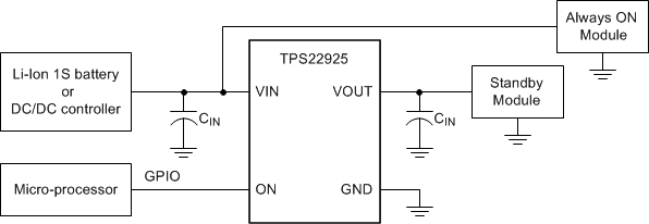
Any end equipment that is being powered from the battery has a need to reduce current consumption in order to maintain the battery charge for a longer time. TPS22925 devices help to accomplish this reduction by turning off the supply to the modules that are in standby state and hence significantly reducing the leakage current overhead of the standby modules.
 Figure 31. Standby Power Reduction
9.1.5 Power Multiplexing
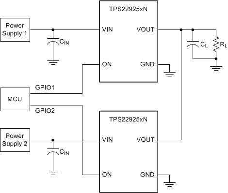
Figure 32 shows a power multiplexing application using two TPS22925xN devices. Use the non-QOD version in order to maintain the output voltage. Configure the GPIO control from the microprocessor unit as break-before-make (BBM).
 Figure 32. Power Multiplexing with Two TPS22925xN Devices
9.1.6 Thermal Considerations
Restrict the maximum junction temperature lower than 125°C. Use Equation 2 to calculate the maximum allowable dissipation, PD(max) for a given output load current and ambient temperature.

where
- PD(max) is the maximum allowable power dissipation
- TJ(max) is the maximum allowable junction temperature
- TA is the ambient temperature of the device
- RθJA is the junction-to-air thermal impedance
NOTE
The RθJA parameter is highly dependent upon board layout. (See the Thermal Information table)
9.2 Typical Application
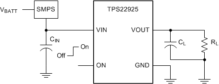
 Figure 33. Typical Application Schematic
9.2.1 Design Requirements
For this design example, use the following as the input parameters.
Table 2. Design Parameters
| DESIGN PARAMETER | EXAMPLE VALUE |
|---|---|
| VIN | 3.6 V |
| CL | 1 µF |
| Maximum Acceptable Inrush Current | 40 mA |
9.2.2 Detailed Design Procedure
9.2.2.1 Managing Inrush Current
When the switch is enabled, the VIN capacitors must be charged up from 0 V to VIN. This charge arrives in the form of inrush current. Calculate the inrush current using Equation 3.

where
- IINRUSH is the inrush current
- CL is the load capacitance
- dv/dt is the output slew rate
TPS22925Bx and TPS22925Cx have different controlled rise time. TPS22925Bx has shorter rise time than TPS22925Cx. In the application where fast rise time is required and higher inrush current can be tolerated, consider using the TPS22925Bx. For an application that requires a longer rise time and lower inrush current, consider using the TPS22925Cx. Calculate the maximum acceptable slew rate using the design requirements and Equation 4.

The TPS22925Bx has a typical rise time of 97 μs at 3.6 V. This results in a slew rate of 29.7 V/ms which meets the above design requirements. The TPS22925Cx has a typical rise time of 810 μs at 3.6 V. This results in a slew rate of 3.6 V/ms which also meets the above design requirements. Base on inrush current requirement, either devices can be used.
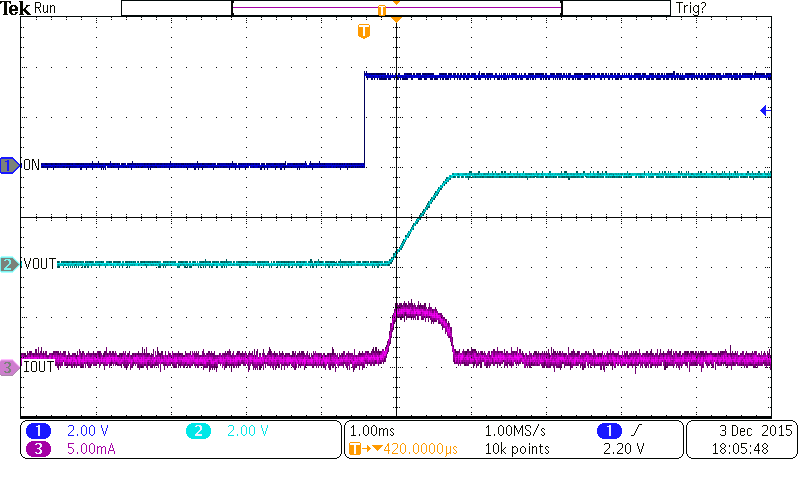
9.2.3 Application Curve

| CL = 1 µF |