ZHCSEX7C November   2015  – February 2016 TPS22925

PRODUCTION DATA.  

  1. 特性
  2. 应用
  3. 说明
  4. 修订历史记录
  5. Device Comparison Table
  6. Pin Configuration and Functions
  7. Specifications
    1. 7.1 Absolute Maximum Ratings
    2. 7.2 ESD Ratings
    3. 7.3 Recommended Operating Conditions
    4. 7.4 Thermal Information
    5. 7.5 Electrical Characteristics
    6. 7.6 Switching Characteristics
    7. 7.7 Typical Characteristics
  8. Detailed Description
    1. 8.1 Overview
    2. 8.2 Functional Block Diagram
    3. 8.3 Feature Description
      1. 8.3.1 ON and OFF Control
      2. 8.3.2 Quick Output Discharge (QOD) (TPS22925B and TPS22925C only)
      3. 8.3.3 Reverse Current Blocking
    4. 8.4 Device Functional Modes
  9. Application and Implementation
    1. 9.1 Application Information
      1. 9.1.1 VIN to VOUT Voltage Drop
      2. 9.1.2 Input Capacitor (CIN)
      3. 9.1.3 Load Capacitor (CL)
      4. 9.1.4 Standby Power Reduction
      5. 9.1.5 Power Multiplexing
      6. 9.1.6 Thermal Considerations
    2. 9.2 Typical Application
      1. 9.2.1 Design Requirements
      2. 9.2.2 Detailed Design Procedure
        1. 9.2.2.1 Managing Inrush Current
      3. 9.2.3 Application Curve
  10. 10Power Supply Recommendations
  11. 11Layout
    1. 11.1 Layout Guidelines
    2. 11.2 Layout Example
  12. 12器件和文档支持
    1. 12.1 社区资源
    2. 12.2 商标
    3. 12.3 静电放电警告
    4. 12.4 Glossary
  13. 13机械、封装和可订购信息

封装选项

机械数据 (封装 | 引脚)
散热焊盘机械数据 (封装 | 引脚)
订购信息

6 Pin Configuration and Functions

YPH Package
6–Pin DSBGA
Top View
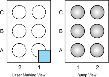
TPS22925 po_slvs840.gif

Pin Assignments

C GND ON
B VOUT VIN
A VOUT VIN
1 2

Pin Functions

PIN TYPE DESCRIPTION
NAME NO.
GND C1 GND Ground
ON C2 I Switch control input. Active high. Do not leave floating.
VIN A2 I Switch input; bypass this input with a ceramic capacitor to ground. See Application Information section for more detail.
B2
VOUT A1 O Switch output
B1