SLIS135E December   2010  – February 2017

PRODUCTION DATA.  

  1. Features
  2. Applications
  3. Description
  4. Revision History
  5. Pin Configuration and Functions
  6. Specifications
    1. 6.1 Absolute Maximum Ratings
    2. 6.2 ESD Ratings
    3. 6.3 Recommended Operating Conditions
    4. 6.4 Thermal Information
    5. 6.5 Electrical Characteristics
    6. 6.6 Operating Characteristics
    7. 6.7 SPI Timing Requirements
    8. 6.8 Typical Characteristics
  7. Detailed Description
    1. 7.1 Overview
    2. 7.2 Functional Block Diagram
    3. 7.3 Feature Description
      1. 7.3.1 Dual Channel, 256-Position Resolution
      2. 7.3.2 Non-Volatile Memory
    4. 7.4 Device Functional Modes
      1. 7.4.1 Voltage Divider Mode
      2. 7.4.2 Rheostat Mode
      3. 7.4.3 Ideal Resistance Values
    5. 7.5 Programming
      1. 7.5.1 SPI Digital Interface
    6. 7.6 Register Map
      1. 7.6.1 Digital Interface Format
      2. 7.6.2 Write-Wiper Register (Command 00)
      3. 7.6.3 Write-NV Register (Command 01)
      4. 7.6.4 Copy Wiper Register to NV Register (Command 10)
      5. 7.6.5 Copy NV Register to Wiper Register (Command 11)
  8. Application and Implementation
    1. 8.1 Application Information
    2. 8.2 Typical Application
      1. 8.2.1 Design Requirements
      2. 8.2.2 Detailed Design Procedure
      3. 8.2.3 Application Curve
  9. Power Supply Recommendations
    1. 9.1 Power Sequence
    2. 9.2 Wiper Position Upon Power Up
  10. 10Layout
    1. 10.1 Layout Guidelines
    2. 10.2 Layout Example
  11. 11Device and Documentation Support
    1. 11.1 Documentation Support
      1. 11.1.1 Related Documentation
    2. 11.2 Receiving Notification of Documentation Updates
    3. 11.3 Community Resources
    4. 11.4 Trademarks
    5. 11.5 Electrostatic Discharge Caution
    6. 11.6 Glossary
  12. 12Mechanical, Packaging, and Orderable Information

封装选项

机械数据 (封装 | 引脚)
散热焊盘机械数据 (封装 | 引脚)
订购信息

Pin Configuration and Functions

RTE Package
16-Pin WQFN With Exposed Thermal Pad
Top View
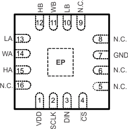
TPL0202 po2_LIS135.gif

Pin Functions

PIN I/O DESCRIPTION
NAME NO.
VDD 1 Power Supply voltage
SCLK 2 Input SPI clock
DIN 3 Input SPI input
CS 4 Input SPI chip select (active low)
N.C. 5, 6, 8, 9, 16 Not internally connected. Can be connected to GND
GND 7 Ground
LB 10 I/O Low terminal of potentiometer B
WB 11 I/O Wiper terminal of potentiometer B
HB 12 I/O High terminal of potentiometer B
LA 13 I/O Low terminal of potentiometer A
WA 14 I/O Wiper terminal of potentiometer A
HA 15 I/O High terminal of potentiometer A
EP EP Exposed thermal pad
Can be connected to GND or left unconnected.