ZHCSQ23E October   2004  – May 2022 TPIC1021

PRODUCTION DATA  

  1. 特性
  2. 应用
  3. 说明
  4. Revision History
  5. 说明(续)
  6. Pin Configuration and Functions
  7. Specifications
    1. 7.1 Absolute Maximum Ratings
    2. 7.2 ESD Ratings
    3. 7.3 Recommended Operating Conditions
    4. 7.4 Thermal Information
    5. 7.5 Electrical Characteristics
    6. 7.6 Timing Requirements
    7. 7.7 Typical Characteristics
  8. Detailed Description
    1. 8.1 Overview
    2. 8.2 Functional Block Diagram
    3. 8.3 Feature Description
      1. 8.3.1 LIN Bus Pin
        1. 8.3.1.1 Transmitter Characteristics
        2. 8.3.1.2 Receiver Characteristics
      2. 8.3.2 Transmit Input Pin (TXD)
        1. 8.3.2.1 TXD Dominant State Timeout
      3. 8.3.3 Receive Output Pin (RXD)
        1. 8.3.3.1 RXD Wake-up Request
      4. 8.3.4 Ground (GND)
      5. 8.3.5 Enable Input Pin (EN)
      6. 8.3.6 NWake Input Pin (NWake)
      7. 8.3.7 Inhibit Output Pin (INH)
    4. 8.4 Device Functional Modes
      1. 8.4.1 Operating States
        1. 8.4.1.1 Normal Mode
        2. 8.4.1.2 Low Power Mode
        3. 8.4.1.3 Wake-Up Events
        4. 8.4.1.4 Standby Mode
      2. 8.4.2 Supply Voltage (VSUP)
  9. Application and Implementation
    1. 9.1 Application Information
    2. 9.2 Typical Application
      1. 9.2.1 Design Requirements
      2. 9.2.2 Detailed Design Procedure
      3. 9.2.3 Application Curves
    3. 9.3 Power Supply Recommendations
    4. 9.4 Layout
      1. 9.4.1 Layout Guidelines
      2. 9.4.2 Layout Example
  10. 10Device and Documentation Support
    1. 10.1 接收文档更新通知
    2. 10.2 支持资源
    3. 10.3 Trademarks
    4. 10.4 Electrostatic Discharge Caution
    5. 10.5 术语表
  11. 11Mechanical, Packaging, and Orderable Information

封装选项

请参考 PDF 数据表获取器件具体的封装图。

机械数据 (封装 | 引脚)
  • D|8
散热焊盘机械数据 (封装 | 引脚)
订购信息

Application Curves

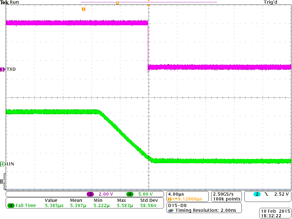
Figure 9-2 and Figure 9-3 show the propagation delay from the TXD pin to the LIN pin for both the recessive to dominant and dominant to recessive states under lightly loaded conditions.
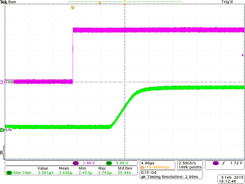
GUID-A14E45B8-FD99-4D5A-BF8E-F1ADA5AB3038-low.pngFigure 9-2 Dominant to Recessive Propagation Delay
GUID-1D3D5E18-A95B-4050-8F26-0C532136AD1E-low.pngFigure 9-3 Recessive to Dominant Propagation Delay