SLLS907E August 2008 – August 2014 TPD4F003 , TPD6F003 , TPD8F003
PRODUCTION DATA.
- 1 Features
- 2 Applications
- 3 Description
- 4 Revision History
- 5 Pin Configuration and Functions
- 6 Specifications
-
7 Detailed Description
- 7.1 Overview
- 7.2 Functional Block Diagram
- 7.3
Feature Description
- 7.3.1 Four-, Six-, and Eight-Channel EMI Filtering for Data Ports
- 7.3.2 -3 dB Bandwidth of 200 MHz
- 7.3.3 Greater Than 25 dB Attenuation at 1 GHz
- 7.3.4 Robust ESD Protection Exceeds IEC 61000-4-2
- 7.3.5 Pi-Style (C-R-C) Filter Configuration
- 7.3.6 Low 10-nA Leakage Current
- 7.3.7 Easy Flow-Through Routing
- 7.4 Device Functional Modes
- 8 Applications and Implementation
- 9 Power Supply Recommendations
- 10Layout
- 11Device and Documentation Support
- 12Mechanical, Packaging, and Orderable Information
封装选项
请参考 PDF 数据表获取器件具体的封装图。
机械数据 (封装 | 引脚)
- DQD|12
散热焊盘机械数据 (封装 | 引脚)
- DQD|12
订购信息
5 Pin Configuration and Functions
DQD PACKAGE
(TOP VIEW)
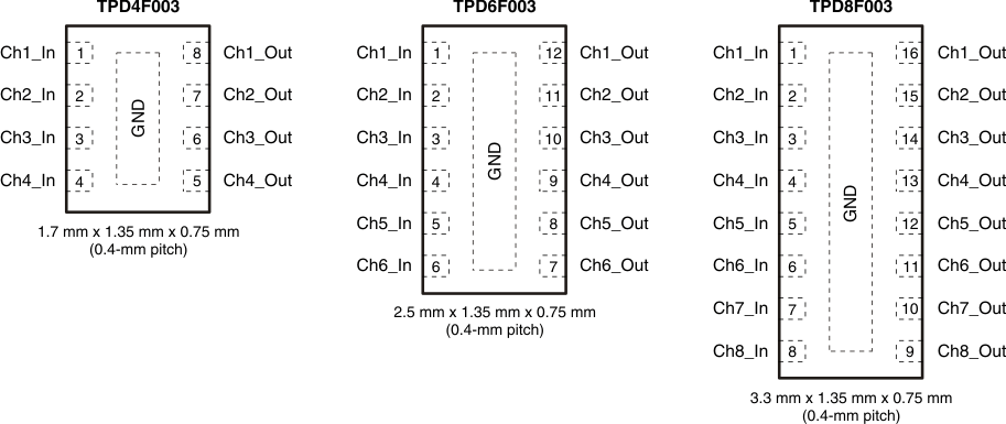
Pin Functions - TPD4F003
| PIN | I/O | DESCRIPTION | |
|---|---|---|---|
| NAME | No. | ||
| ChX_In | 1, 2, 3, 4 | IO | ESD-protected channel, connected to corresponding ChX_Out |
| ChX_Out | 5, 6, 7, 8 | IO | ESD-protected channel, connected to corresponding ChX_In |
| GND | GND | G | Ground |
Pin Functions - TPD6F003
| PIN | I/O | Description | |
|---|---|---|---|
| Name | No. | ||
| ChX_In | 1, 2, 3, 4, 5, 6 | IO | ESD-protected channel, connected to corresponding ChX_Out |
| ChX_Out | 7, 8, 9, 10, 11, 12 | IO | ESD-protected channel, connected to corresponding ChX_In |
| GND | GND | G | Ground |
Pin Functions - TPD8F003
| PIN | I/O | Description | |
|---|---|---|---|
| Name | No. | ||
| ChX_In | 1, 2, 3, 4, 5, 6, 7, 8 | IO | ESD-protected channel, connected to corresponding ChX_Out |
| ChX_Out | 9, 10, 11, 12, 13, 14, 15, 16 | IO | ESD-protected channel, connected to corresponding ChX_In |
| GND | GND | G | Ground |