SLLS907E August 2008 – August 2014 TPD4F003 , TPD6F003 , TPD8F003
PRODUCTION DATA.
- 1 Features
- 2 Applications
- 3 Description
- 4 Revision History
- 5 Pin Configuration and Functions
- 6 Specifications
-
7 Detailed Description
- 7.1 Overview
- 7.2 Functional Block Diagram
- 7.3
Feature Description
- 7.3.1 Four-, Six-, and Eight-Channel EMI Filtering for Data Ports
- 7.3.2 -3 dB Bandwidth of 200 MHz
- 7.3.3 Greater Than 25 dB Attenuation at 1 GHz
- 7.3.4 Robust ESD Protection Exceeds IEC 61000-4-2
- 7.3.5 Pi-Style (C-R-C) Filter Configuration
- 7.3.6 Low 10-nA Leakage Current
- 7.3.7 Easy Flow-Through Routing
- 7.4 Device Functional Modes
- 8 Applications and Implementation
- 9 Power Supply Recommendations
- 10Layout
- 11Device and Documentation Support
- 12Mechanical, Packaging, and Orderable Information
封装选项
请参考 PDF 数据表获取器件具体的封装图。
机械数据 (封装 | 引脚)
- DQD|12
散热焊盘机械数据 (封装 | 引脚)
- DQD|12
订购信息
8 Applications and Implementation
8.1 Application Information
The TPDxF003 family are diode type TVS' integrated with series resistors for filtering emitted EMI. As signal passes through the device, higher frequency components are filtered out. This device also provides a path to ground during ESD events and isolates the protected IC. As the current from ESD passes through the TVS, only a small voltage drop is present across the diode. This is the voltage presented to the protected IC. In particular, these filters are ideal for EMI filtering and protecting data lines from ESD at the display, keypad, and memory interfaces.
8.2 Typical Application
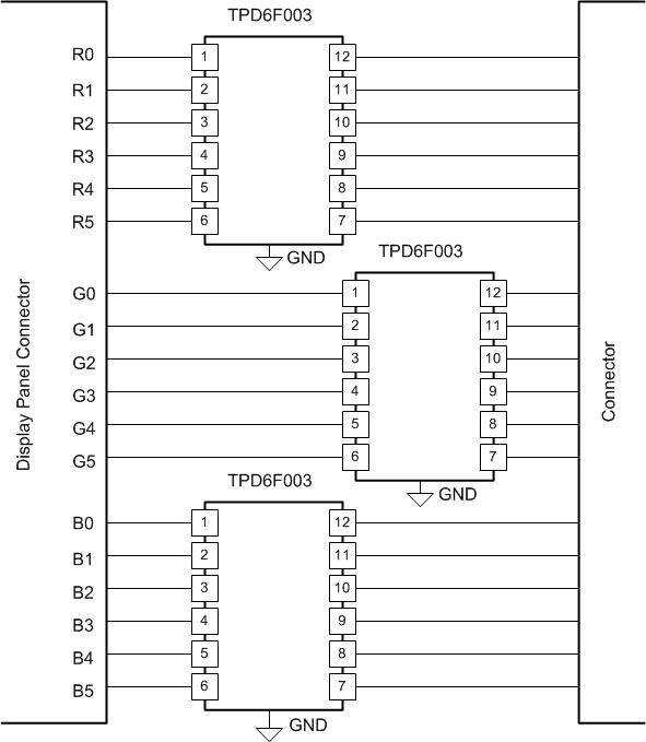 Figure 10. Display Panel Schematic
8.2.1 Design Requirements
For this design example, three TPD6F003 devices are used in an 18-bit display panel application. This will provide a complete ESD and EMI protection solution for the display connector.
Given the display panel application, the following parameters are known.
| DESIGN PARAMETER | VALUE |
|---|---|
| Signal range on all pins except GND | 0 V to 5 V |
| Operating Frequency | 100 MHz |
8.2.2 Detailed Design Procedure
To begin the design process, some design parameters must be decided; the designer need to know the following:
- Signal range on all the protected lines
- Operating frequency
8.2.2.1 Signal Range on All Protected Lines
The TPD6F003 has 8 identical protection channels for signal lines. All I/O pins will support a signal range from 0 to 5.5 V.
8.2.2.2 Operating Frequency
The TPD6F003 has a 200 MHz –3dB bandwidth, which supports the operating frequency for this display.
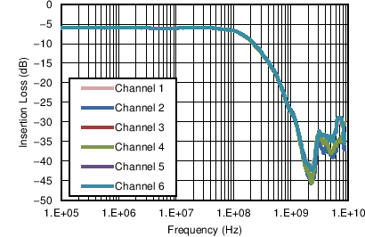
8.2.3 Application Curve