ZHCSSO7C february   2008  – july 2023 TPD6E004

PRODUCTION DATA  

  1.   1
  2. 特性
  3. 应用
  4. 说明
  5. Revision History
  6. Pin Configuration and Functions
  7. Specifications
    1. 6.1 Absolute Maximum Ratings #GUID-506F33E9-2D36-4FA4-A00D-A85E2C505B35/SLLS7994401
    2. 6.2 ESD Ratings
    3. 6.3 ESD Ratings – Surge Protection
    4. 6.4 Recommended Operating Conditions
    5. 6.5 Thermal Information
    6. 6.6 Electrical Characteristics
    7. 6.7 Typical Characteristics
  8. Detailed Description
    1. 7.1 Overview
    2. 7.2 Functional Block Diagram
    3. 7.3 Feature Description
    4. 7.4 Device Functional Modes
  9. Application and Implementation
    1. 8.1 Application Information
    2. 8.2 Typical Application
      1. 8.2.1 Design Requirements
      2. 8.2.2 Detailed Design Procedure
      3. 8.2.3 Application Curve
    3. 8.3 Power Supply Recommendations
    4. 8.4 Layout
      1. 8.4.1 Layout Guidelines
      2. 8.4.2 Layout Example
  10. Device and Documentation Support
    1. 9.1 Documentation Support
      1. 9.1.1 Related Documentation
    2. 9.2 支持资源
    3. 9.3 Trademarks
    4. 9.4 静电放电警告
    5. 9.5 术语表
  11. 10Mechanical, Packaging, and Orderable Information

封装选项

机械数据 (封装 | 引脚)
散热焊盘机械数据 (封装 | 引脚)
订购信息

Pin Configuration and Functions

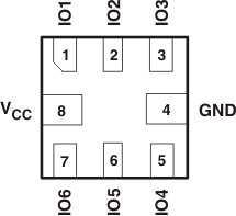
GUID-EC17841B-4E88-4854-A22A-E9202169C094-low.gif Figure 5-1 RSE Package, 8-Pin UQFN (Bottom View)
Table 5-1 Pin Functions
PIN TYPE(1) DESCRIPTION
NAME NO.
IO1 1 I/O ESD-protected channel
IO2 2 I/O ESD-protected channel
IO3 3 I/O ESD-protected channel
GND 4 GND Ground
IO4 5 I/O ESD-protected channel
IO5 6 I/O ESD-protected channel
IO6 7 I/O ESD-protected channel
VCC 8 PWR Power-supply input. Bypass VCC to GND with a 0.1-μF ceramic capacitor.
I = input, O = output, GND = ground, PWR = power