ZHCSCE8F April 2014 – May 2019
PRODUCTION DATA.
- 1 特性
- 2 应用
- 3 说明
- 4 修订历史记录
- 5 Device Comparison Table
- 6 Pin Configuration and Functions
-
7 Specifications
- 7.1 Absolute Maximum Ratings
- 7.2 ESD Ratings
- 7.3 Recommended Operating Conditions
- 7.4 Thermal Information
- 7.5 Supply Current Consumption
- 7.6 Electrical Characteristics EN Pin
- 7.7 Thermal Shutdown Feature
- 7.8 Electrical Characteristics nFET Switch
- 7.9 Electrical Characteristics OVP Circuit
- 7.10 Electrical Characteristics VBUS_POWER Circuit
- 7.11 Timing Requirements
- 7.12 TPD1S514-1 Typical Characteristics
-
8 Detailed Description
- 8.1 Overview
- 8.2 Functional Block Diagram
- 8.3
Feature Description
- 8.3.1 Over Voltage Protection on VBUS_CON up to 30 V DC
- 8.3.2 Precision OVP (< ±1% Tolerance)
- 8.3.3 Low RON nFET Switch Supports Host and Charging Mode
- 8.3.4 VBUS_POWER, TPD1S514-1, TPD1S514-2, TPD1S514-3
- 8.3.5 VBUS_POWER, TPD1S514
- 8.3.6 Powering the System When Battery is Discharged
- 8.3.7 ±15 kV IEC 61000-4-2 Level 4 ESD Protection
- 8.3.8 100 V IEC 61000-4-5 µs Surge Protection
- 8.3.9 Startup and OVP Recovery Delay
- 8.3.10 Thermal Shutdown
- 8.4 Device Functional Modes
- 9 Application and Implementation
- 10Power Supply Recommendations
- 11Layout
- 12器件和文档支持
- 13机械、封装和可订购信息
11.2 Layout Example

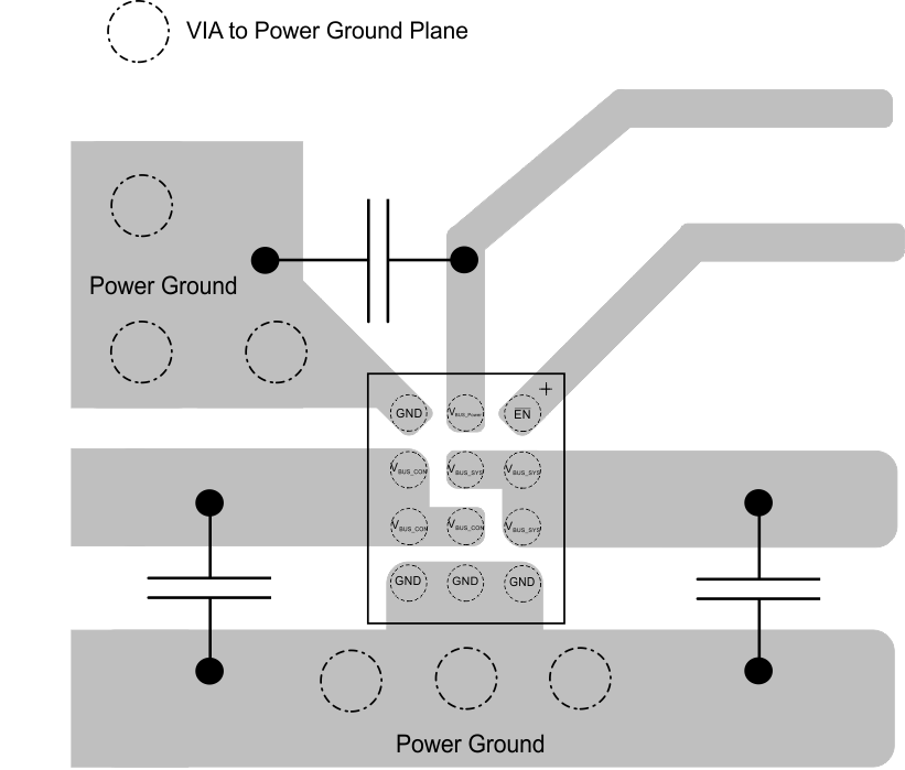
When designing layout for the TPD1S514 Family, note that VBUS_CON and VBUS_SYS pins allow extra wide traces for good power delivery. In the example shown, these pins are routed with 50 mil (1.27 mm) wide traces. Place the VBUS_CON, VBUS_SYS, and VBUS_POWER capacitors as close to the pins as possible. Use external and internal ground planes and stitch them together with VIAs as close to the GND pins of TPD1S514 as possible. This allows for a low impedance path to ground so that the device can properly dissipate any surge or ESD events.
Figure 15. Layout Recommendation