ZHCS404F September 2011 – October 2015 TPD12S016
PRODUCTION DATA.
- 1 特性
- 2 应用范围
- 3 说明
- 4 修订历史记录
- 5 Pin Configuration and Functions
- 6 Specifications
-
7 Detailed Description
- 7.1 Overview
- 7.2 Functional Block Diagram
- 7.3
Feature Description
- 7.3.1 Conforms to HDMI Compliance Tests Without any External Components
- 7.3.2 IEC 61000-4-2 ESD Protection
- 7.3.3 Supports HDMI 1.4 Data Rate
- 7.3.4 Matches Class D and Class C Pin Mapping
- 7.3.5 8-Channel ESD Lines for Four Differential Pairs with Ultra-low Differential Capacitance Matching (0.05 pF)
- 7.3.6 On-Chip Load Switch With 55-mA Current Limit Feature at the HDMI 5V_OUT Pin
- 7.3.7 Auto-direction Sensing I2C Level Shifter With One-Shot Circuit to Drive a Long HDMI Cable (750-pF Load)
- 7.3.8 Back-Drive Protection on HDMI Connector Side Ports
- 7.3.9 Integrated Pullup and Pulldown Resistors per HDMI Specification
- 7.3.10 Space Saving 24-Pin RKT Package and 24-TSSOP Package
- 7.3.11 DDC/CEC LEVEL SHIFT Circuit Operation
- 7.3.12 DDC/CEC Level Shifter Operational Notes For VCCA = 1.8 V
- 7.3.13 Rise-Time Accelerators
- 7.3.14 Noise Considerations
- 7.3.15 Resistor Pullup Value Selection
- 7.4 Device Functional Modes
- 8 Application and Implementation
- 9 Power Supply Recommendations
- 10Layout
- 11器件和文档支持
- 12机械、封装和可订购信息
封装选项
请参考 PDF 数据表获取器件具体的封装图。
机械数据 (封装 | 引脚)
- RKT|24
- PW|24
散热焊盘机械数据 (封装 | 引脚)
- RKT|24
订购信息
7 Detailed Description
7.1 Overview
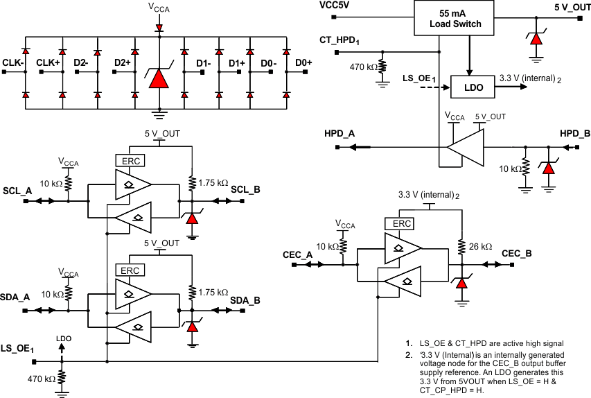
The TPD12S016 is a single-chip HDMI interface device with auto-direction sensing I2C voltage level shifting buffers, a load switch, and integrated high-speed ESD protection clamps. The device pin mapping matches the HDMI connector with four differential pairs and control lines. This device offers eight low-capacitance ESD clamps, allowing HDMI 1.4 data rates. The integrated ESD circuits provides matching between each differential signal pair, which allows an advantage over discrete ESD solutions where variations between ESD protection clamps degrade the differential signal quality. The TPD12S016 provides a current limited 5-V output (5V_OUT) for sourcing the HDMI power line. The current limited 5-V output supplies up to 55 mA to the HDMI receiver. The control of 5V_OUT and the hot plug detect (HPD) circuitry is independent of the LS_OE control signal, and is controlled by the CT_HPD pin. This independent CT_HPD control enables the detection scheme (5V_OUT and HPD) to be active before enabling the HDMI link. An internal 3.3 V node powers the CEC pin eliminating the need for a 3.3 V supply on board.
The TPD12S016 integrates all the external termination resistors at the HPD, CEC, SCL, and SDA lines. There are three non-inverting bidirectional voltage level translation (VLT) circuits for the SDA, SCL, and CEC lines. Each have a common power rail (VCCA) on the A side from 1.1 V to 3.6V. On the B side, the SCL_B and SDA_B each have an internal 1.75 kΩ pull up connected to the 5-V rail (5V_OUT). The SCL and SDA pins meet the I2C specification and drive up to 750-pF capacitive loads exceeding the HDMI 1.4 specifications. The CEC_B pin has an internal 27-kΩ pull up resistor to the internal 3.3-V supply rail. The HPD_B port has a glitch filter to avoid false detection due to plug bouncing during the HDMI connector insertion.
The TPD12S016 offers a reverse current blocking feature at the 5V_OUT pin. In the fault conditions, such as when two HDMI transmitters connect to the same HDMI cable, the TPD12S016 ensures that the system is safe from powering up through an external HDMI transmitter. The SCL_B, SDA_B, CEC_B pins also feature reverse-current blocking when the system is powered off.
7.3 Feature Description
7.3.1 Conforms to HDMI Compliance Tests Without any External Components
The TPD12S016 has integrated pullup or pulldown resistors on the DDC, CEC, and HPD lines that conform to the HDMI 7.13 and 7.15 Compliance Tests without the designer needing to use any external components to TPD12S016.
7.3.2 IEC 61000-4-2 ESD Protection
In many cases, the core ICs, such as the scalar chipset, may not have robust ESD cells to sustain system-level ESD strikes. In these cases, the TPD12S016 provides the desired system-level ESD protection, such as the IEC 61000-4-2 Level 4 ESD protection of ±8-kV Contact rating by absorbing the energy associated with the ESD strike.
7.3.3 Supports HDMI 1.4 Data Rate
The high-speed TMDS pins of the TPD12S016 add only 1.0-pF (for PW package) or 1.2-pF (for RKT package) of capacitance to the TMDS lines. An Insertion Loss –3 dB point that is greater than 3 GHz provides enough bandwidth to pass HDMI 1.4 TMDS data rates.
7.3.4 Matches Class D and Class C Pin Mapping
The PW and RKT packages offer seamless layout routing options to eliminate the routing glitch for the differential signal pairs. The pin mapping follows the same order as the HDMI connector pin mapping.
7.3.5 8-Channel ESD Lines for Four Differential Pairs with Ultra-low Differential Capacitance Matching (0.05 pF)
Excellent intra-pair capacitance matching of 0.05 pF provides ultra low intra-pair skew, which allows an advantage over discrete ESD solutions where variations between ESD protection clamps can degrade the differential signal quality.
7.3.6 On-Chip Load Switch With 55-mA Current Limit Feature at the HDMI 5V_OUT Pin
The TPD12S016 provides a current limited 5-V output (5V_OUT) for sourcing the HDMI power line. The current limited 5-V output supplies up to 55 mA to the HDMI receiver. The control of 5V_OUT and the HPD circuitry is independent of the LS_OE control signal, and is controlled by the CT_HPD pin. This independent CT_HPD control enables the detection scheme (5V_OUT and HPD) to be active before enabling the HDMI link.
7.3.7 Auto-direction Sensing I2C Level Shifter With One-Shot Circuit to Drive a Long HDMI Cable (750-pF Load)
The TPD12S016 contains three bidirectional open-drain buffers specifically designed to support up-translation/down-translation between the low voltage, VCCA side DDC-bus and the 5-V DDC-bus or 3.3-V CEC line. The HDMI cable side of the DDC lines incorporates rise-time accelerators to support a high capacitive load on the HDMI cable side. The rise time accelerators boost the cable side DDC signal independent of which side of the bus is releasing the signal.
7.3.8 Back-Drive Protection on HDMI Connector Side Ports
The TPD12S016 offers a reverse current blocking feature at the 5V_OUT pin. In fault conditions, such as when two HDMI transmitters connect to the same HDMI cable, the TPD12S016 ensures that the system is safe from powering up through an external HDMI transmitter. The SCL_B, SDA_B, CEC_B pins also feature reverse-current blocking when the system is powered off.
7.3.9 Integrated Pullup and Pulldown Resistors per HDMI Specification
The system is designed to work properly according to the HDMI 1.4 specification with no external pullup resistors on the DDC, CEC, and HPD lines.
7.3.10 Space Saving 24-Pin RKT Package and 24-TSSOP Package
When compared to discrete ESD solutions, the fully integrated port protection offered by TPD12S016 reduces the overall area required to fully protect an HDMI transmitter port.
7.3.11 DDC/CEC LEVEL SHIFT Circuit Operation
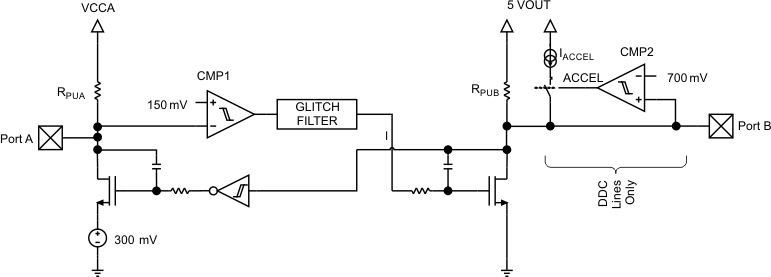
The TPD12S016 enables DDC translation from VCCA (system side) voltage levels to 5-V (HDMI cable side) voltage levels without degradation of system performance. The TPD12S016 contains two bidirectional open-drain buffers specifically designed to support up-translation/down-translation between the low voltage, VCCA side DDC-bus and the 5-V DDC-bus. The port B I/Os are over-voltage tolerant to 5.5 V, even when the device is un-powered. After power-up and with the LS_OE and CT_HPD pins HIGH, a LOW level on port A (below approximately VILC = 0.08 × VCCA V) turns the corresponding port B driver (either SDA or SCL) on and drives port B down to VOLB V. When port A rises above approximately 0.10 × VCCA V, the port B pulldown driver is turned off and the internal pullup resistor pulls the pin HIGH. When port B falls first and goes below 0.3 × 5 VOUT V, a CMOS hysteresis input buffer detects the falling edge, turns on the port A driver, and pulls port A down to approximately VOLA = 0.16 × VCCA V. The port B pulldown is not enabled unless the port A voltage goes below VILC. If the port A low voltage goes below VILC, the port B pulldown driver is enabled until port A rises above (VILC + ΔVT-HYSTA), then port B, if not externally driven LOW, will continue to rise being pulled up by the internal pullup resistor.
 Figure 13. DDC/CEC Level Shifter Block Diagram
7.3.12 DDC/CEC Level Shifter Operational Notes For VCCA = 1.8 V
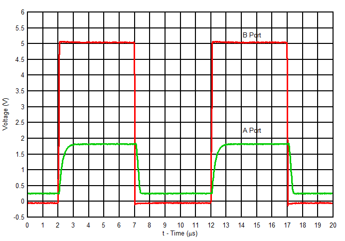
- The threshold of CMP1 (see Figure 13) is approximately 150 mV ± the 40 mV of total hysteresis.
- The comparator will trip for a falling waveform at approximately 130 mV.
- The comparator will trip for a rising waveform at approximately 170 mV.
- To be recognized as a zero, the level at Port A must first go below 130 mV (VILC in spec) and then stay below 170 mV (VILA in spec).
- To be recognized as a one, the level at A must first go above 170 mV and then stay above 130 mV.
- VILC is set to 117 mV in Electrical Characteristics Table to give some margin to the 130 mV.
- VILA is set to 148 mV in the Electrical Characteristics table to give some margin to the 170 mV.
- VIHA is set to 70% of VCCA to be consistent with standard CMOS levels.
 Figure 14. DDC Level Shifter Operation (B To A Direction)
7.3.13 Rise-Time Accelerators
The HDMI cable side of the DDC lines incorporates rise-time accelerators to support high capacitive load (up to 750 pF) on the HDMI cable side. The rise time accelerators boost the cable side DDC signal independent of which side of the bus is releasing the signal.
7.3.14 Noise Considerations
Ground offset between the TPD12S016 ground and the ground of devices on port A of the TPD12S016 must be avoided. The reason for this cautionary remark is that a CMOS/NMOS open-drain capable of sinking 3 mA of current at 0.4 V will have an output resistance of 133 Ω or less (R = E / I). Such a driver will share enough current with the port A output pulldown of the TPD12S016 to be seen as a LOW as long as the ground offset is zero. If the ground offset is greater than 0 V, then the driver resistance must be less. Since VILC can be as low as 90 mV at cold temperatures and the low end of the current distribution, the maximum ground offset should not exceed 50 mV. Bus repeaters that use an output offset are not interoperable with the port A of the TPD12S016 as their output LOW levels will not be recognized by the TPD12S016 as a LOW. If the TPD12S016 is placed in an application where the VIL of port A of the TPD12S016 does not go below its VILC it will pull port B LOW initially when port A input transitions LOW but the port B will return HIGH, so it will not reproduce the port A input on port B. Such applications should be avoided. Port B is interoperable with all I2C-bus slaves, masters and repeaters.
7.3.15 Resistor Pullup Value Selection
The system is designed to work properly with no external pullup resistors on the DDC, CEC, and HPD lines.
7.4 Device Functional Modes
The LS_OE and CT_HPD are active-high enable pins. They control the TPD12S016 power saving options according to Table 1.
Table 1. Power Saving Options(1)
| LS_OE | CT_HPD | VCCA | VCC5V | A-SIDE PULL-UPS |
DDC, B-SIDE PULL-UPS |
CEC_B PULL-UPS |
CEC LDO |
LOAD SW AND HPD |
DDC/ CEC VLTs |
ICCA TYP |
ICC5V TYP |
COMMENTS |
|---|---|---|---|---|---|---|---|---|---|---|---|---|
| L | L | 1.8 V | 5.0 V | Off | Off | Off | Off | Off | Off | 1 µA | 1 µA | Fully Disabled |
| L | H | 1.8 V | 5.0 V | On | On | Off | Off | On | Off | 1 µA | 30 µA | Load Switch on |
| H | L | 1.8 V | 5.0 V | Off | Off | Off | Off | Off | Off | 1 µA | 1 µA | Not a Valid State |
| H | H | 1.8 V | 5.0 V | On | On | On | On | On | On | 13 µA | 200 µA | Fully On |
| X | X | 0 V | 0 V | High-Z | High-Z | High-Z | Off | Off | Off | 0 | 0 | Power Down |
| X | X | 1.8 V | 0 V | High-Z | High-Z | High-Z | Off | Off | Off | 0 | 0 | Power Down |
| X | X | 0 V | 5.0 V | High-Z | High-Z | High-Z | Off | Off | Off | 0 | 0 | Power Down |
