ZHCSHB1B January   2018  – August 2018 TPA3220

PRODUCTION DATA.  

  1. 特性
  2. 应用
  3. 说明
    1.     简化原理图
  4. 修订历史记录
  5. Device Comparison Table
  6. Pin Configuration and Functions
    1.     Pin Functions
  7. Specifications
    1. 7.1 Absolute Maximum Ratings
    2. 7.2 ESD Ratings
    3. 7.3 Recommended Operating Conditions
    4. 7.4 Thermal Information
    5. 7.5 Electrical Characteristics
    6. 7.6 Audio Characteristics (BTL)
    7. 7.7 Audio Characteristics (PBTL)
    8. 7.8 Typical Characteristics, BTL Configuration, AD-mode
    9. 7.9 Typical Characteristics, PBTL Configuration, AD-mode
  8. Parameter Measurement Information
  9. Detailed Description
    1. 9.1 Overview
    2. 9.2 Functional Block Diagrams
    3. 9.3 Feature Description
      1. 9.3.1 Internal LDO
        1. 9.3.1.1 Input Configuration, Gain Setting And Master / Slave Operation
      2. 9.3.2 Gain Setting And Master / Slave Operation
      3. 9.3.3 AD-Mode and HEAD-Mode PWM Modulation
      4. 9.3.4 Oscillator
      5. 9.3.5 Input Impedance
      6. 9.3.6 Error Reporting
    4. 9.4 Device Functional Modes
      1. 9.4.1 Powering Up
        1. 9.4.1.1 Startup Ramp Time
      2. 9.4.2 Powering Down
        1. 9.4.2.1 Power Down Ramp Time
      3. 9.4.3 Device Reset
      4. 9.4.4 Device Soft Mute
      5. 9.4.5 Device Protection System
        1. 9.4.5.1 Overload and Short Circuit Current Protection
        2. 9.4.5.2 Signal Clipping and Pulse Injector
        3. 9.4.5.3 DC Speaker Protection
        4. 9.4.5.4 Pin-to-Pin Short Circuit Protection (PPSC)
        5. 9.4.5.5 Overtemperature Protection OTW and OTE
        6. 9.4.5.6 Undervoltage Protection (UVP) and Power-on Reset (POR)
        7. 9.4.5.7 Fault Handling
  10. 10Application and Implementation
    1. 10.1 Application Information
    2. 10.2 Typical Applications
      1. 10.2.1 Stereo BTL Application
        1. 10.2.1.1 Design Requirements
        2. 10.2.1.2 Detailed Design Procedures
          1. 10.2.1.2.1 Decoupling Capacitor Recommendations
          2. 10.2.1.2.2 PVDD Capacitor Recommendation
          3. 10.2.1.2.3 BST capacitors
          4. 10.2.1.2.4 PCB Material Recommendation
      2. 10.2.2 Typical Application, Differential (2N), AD-Mode PBTL (Outputs Paralleled before LC filter)
        1. 10.2.2.1 Design Requirements
      3. 10.2.3 Typical Application, Differential (2N), AD-Mode PBTL (Outputs Paralleled after LC filter)
        1. 10.2.3.1 Design Requirements
  11. 11Power Supply Recommendations
    1. 11.1 Power Supplies
      1. 11.1.1 VDD Supply
      2. 11.1.2 AVDD and GVDD Supplies
      3. 11.1.3 PVDD Supply
      4. 11.1.4 BST Supply
  12. 12Layout
    1. 12.1 Layout Guidelines
    2. 12.2 Layout Examples
      1. 12.2.1 BTL Application Printed Circuit Board Layout Example
      2. 12.2.2 PBTL (Outputs Paralleled before LC filter) Application Printed Circuit Board Layout Example
      3. 12.2.3 PBTL (Outputs Paralleled after LC filter) Application Printed Circuit Board Layout Example
  13. 13器件和文档支持
    1. 13.1 文档支持
    2. 13.2 接收文档更新通知
    3. 13.3 社区资源
    4. 13.4 商标
    5. 13.5 静电放电警告
    6. 13.6 术语表
  14. 14机械、封装和可订购信息

封装选项

请参考 PDF 数据表获取器件具体的封装图。

机械数据 (封装 | 引脚)
  • DDW|44
散热焊盘机械数据 (封装 | 引脚)
订购信息

Typical Characteristics, BTL Configuration, AD-mode

All Measurements taken at audio frequency = 1 kHz, PVDD_X = 30 V, VDD = 5 V, GVDD = 5 V, RL = 4 Ω, fS = 480 kHz, TA = 25°C, Output Filter: LDEM = 10 μH, CDEM = 1 µF, AD Modulation, AES17 + AUX-0025 measurement filters, unless otherwise noted.
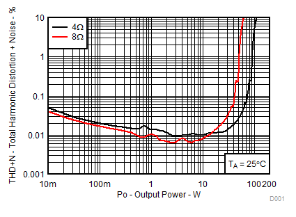
TPA3220 D001_SLASEN3.gif
RL = 3 Ω, 4 Ω, 8 Ω TA = 25°C
Figure 1. Total Harmonic Distortion + Noise vs Output Power, AD-mode
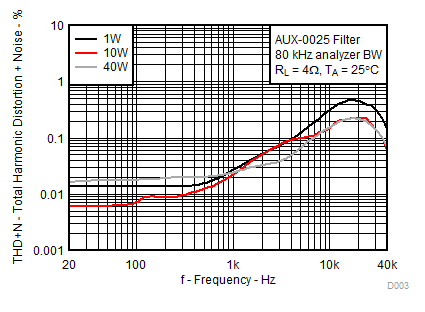
TPA3220 D003_SLASEN3.gif
RL =4 Ω P = 1W, 10W, 40W
AUX-0025 filter, 80 kHz analyzer BW TA = 25°C
Figure 3. Total Harmonic Distortion+Noise vs Frequency, AD-mode
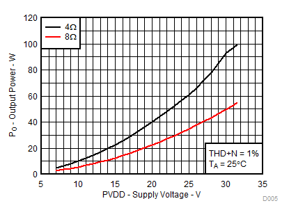
TPA3220 D005_SLASEN3.gif
RL = 4 Ω, 8 Ω THD+N = 1%
Figure 5. Output Power vs Supply Voltage, AD-mode
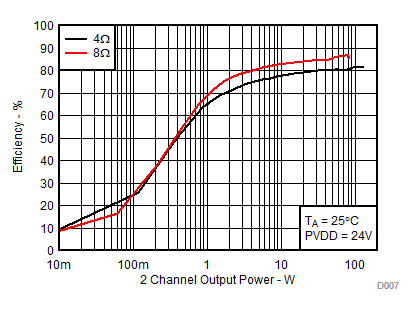
TPA3220 D007_SLASEN3.gif
RL = 4 Ω, 8 Ω PVDD = 24V
Figure 7. System Efficiency vs Output Power, AD-mode
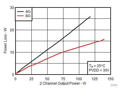
TPA3220 D009_SLASEN3.gif
RL = 4 Ω, 8 Ω
Figure 9. System Power Loss vs Output Power, AD-mode
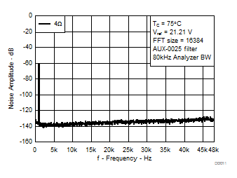
TPA3220 D011_SLASEE9.gif
RL = 4 Ω
Figure 11. Noise Amplitude vs Frequency, AD-mode
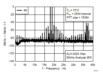
TPA3220 D013_SLASEE9.gif
Figure 13. CCIF Intermodulation, AD-Mode, 25 W
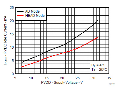
TPA3220 D026_SLASEN3.gif
Figure 15. Idle Current vs Supply Voltage, AD vs HEAD
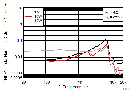
TPA3220 D002_SLASEN3.gif
RL = 4 Ω P = 1W, 10W, 40W TA = 25°C
Figure 2. Total Harmonic Distortion+Noise vs Frequency, AD-mode
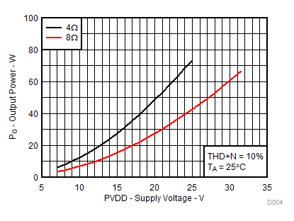
TPA3220 D004_SLASEN3.gif
RL = 4 Ω, 8 Ω THD+N = 10%
Figure 4. Output Power vs Supply Voltage, AD-mode
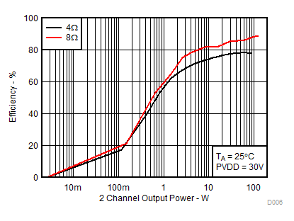
TPA3220 D006_SLASEN3.gif
RL = 4 Ω, 8 Ω PVDD = 30V
Figure 6. System Efficiency vs Output Power, AD-mode
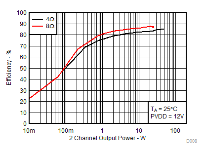
TPA3220 D008_SLASEN3.gif
RL = 4 Ω, 8 Ω PVDD = 12V
Figure 8. System Efficiency vs Output Power, AD-mode
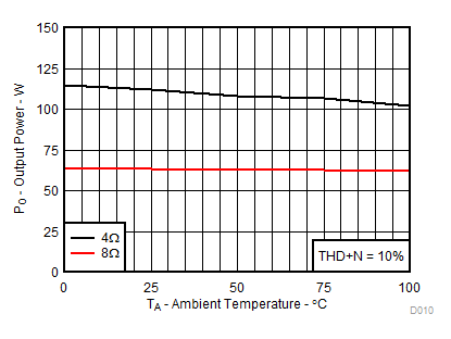
TPA3220 D010_SLASEN3.gif
RL = 4 Ω, 8 Ω
Figure 10. Output Power vs Ambient Temperature, AD-mode
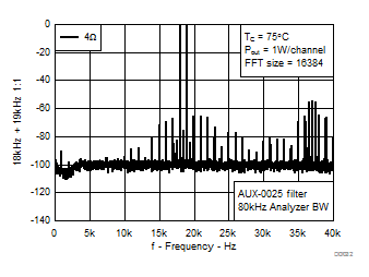
TPA3220 D012_SLASEE9.gif
18 kHz + 19 kHz Ratio 1 : 1
Figure 12. CCIF Intermodulation, AD-mode, 1 W
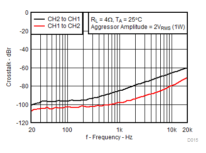
TPA3220 D015_SLASEN3.gif
Figure 14. Channel-to-Channel Crosstalk vs Frequency, AD-mode
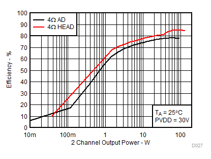
TPA3220 D027_4_SLASEN3.gif
Figure 16. Efficiency vs Output Power, AD vs HEAD