ZHCS891G April 2012 – December 2017 TPA3116D2 , TPA3118D2 , TPA3130D2
PRODUCTION DATA.
- 1 特性
- 2 应用
- 3 说明
- 4 修订历史记录
- 5 Pin Configuration and Functions
- 6 Specifications
-
7 Detailed Description
- 7.1 Overview
- 7.2 Functional Block Diagram
- 7.3
Feature Description
- 7.3.1 Gain Setting and Master and Slave
- 7.3.2 Input Impedance
- 7.3.3 Startup and Shutdown Operation
- 7.3.4 PLIMIT Operation
- 7.3.5 GVDD Supply
- 7.3.6 BSPx AND BSNx Capacitors
- 7.3.7 Differential Inputs
- 7.3.8 Device Protection System
- 7.3.9 DC Detect Protection
- 7.3.10 Short-Circuit Protection and Automatic Recovery Feature
- 7.3.11 Thermal Protection
- 7.3.12 Device Modulation Scheme
- 7.3.13 Efficiency: LC Filter Required with the Traditional Class-D Modulation Scheme
- 7.3.14 Ferrite Bead Filter Considerations
- 7.3.15 When to Use an Output Filter for EMI Suppression
- 7.3.16 AM Avoidance EMI Reduction
- 7.4 Device Functional Modes
- 8 Application and Implementation
- 9 Power Supply Recommendations
- 10Layout
- 11器件和文档支持
- 12机械、封装和可订购信息
7.3.15 When to Use an Output Filter for EMI Suppression
The TPA3116D2 has been tested with a simple ferrite bead filter for a variety of applications including long speaker wires up to 125 cm and high power. The TPA3116D2 EVM passes FCC class-B specifications under these conditions using twisted speaker wires. The size and type of ferrite bead can be selected to meet application requirements. Also, the filter capacitor can be increased if necessary with some impact on efficiency.
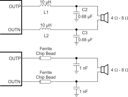
There may be a few circuit instances where it is necessary to add a complete LC reconstruction filter. These circumstances might occur if there are nearby circuits which are sensitive to noise. In these cases a classic second order Butterworth filter similar to those shown in the figures below can be used.
Some systems have little power supply decoupling from the AC line but are also subject to line conducted interference (LCI) regulations. These include systems powered by "wall warts" and "power bricks." In these cases, LC reconstruction filters can be the lowest cost means to pass LCI tests. Common mode chokes using low frequency ferrite material can also be effective at preventing line conducted interference.
 Figure 35. TPA31xxD2 Output Filters