ZHCSAA4B September 2012 – September 2015 TPA3110D2-Q1
PRODUCTION DATA.
- 1 特性
- 2 应用
- 3 说明
- 4 修订历史记录
- 5 Pin Configuration and Functions
- 6 Specifications
- 7 Detailed Description
-
8 Application and Implementation
- 8.1 Application Information
- 8.2
Typical Application
- 8.2.1 Design Requirements
- 8.2.2
Detailed Design Procedure
- 8.2.2.1 TPA3110D2-Q1 Modulation Scheme
- 8.2.2.2 Ferrite Bead Filter Considerations
- 8.2.2.3 Efficiency: LC Filter Required With the Traditional Class-D Modulation Scheme
- 8.2.2.4 When to Use an Output Filter for EMI Suppression
- 8.2.2.5 Input Resistance
- 8.2.2.6 Input Capacitor, CI
- 8.2.2.7 BSN and BSP Capacitors
- 8.2.2.8 Differential Inputs
- 8.2.2.9 Using Low-ESR Capacitors
- 8.2.3 Application Curve
- 9 Power Supply Recommendations
- 10Layout
- 11器件和文档支持
- 12机械、封装和可订购信息
7.4.4 PLIMIT
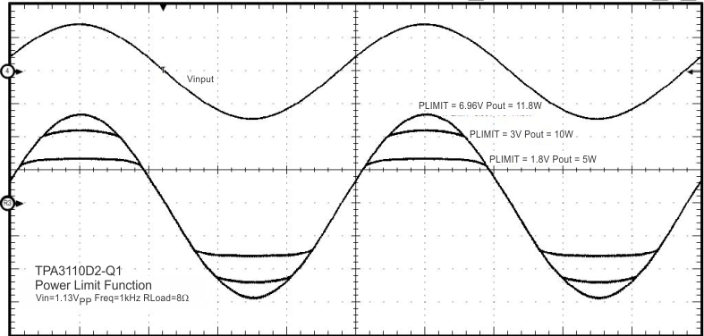
The PLIMIT pin limits the output peak-to-peak voltage based on the voltage supplied to the PLIMIT pin. The peak output voltage is limited to four times the voltage at the PLIMIT pin.
 Figure 35. PLIMIT Circuit Operation
The PLIMIT circuit sets a limit on the output peak-to-peak voltage. The limiting is done by limiting the duty cycle to fixed maximum value. This limit can be thought of as a virtual voltage rail which is lower than the supply connected to PVCC. This virtual rail is four times the voltage at the PLIMIT pin. This output voltage can be used to calculate the maximum output power for a given maximum input voltage and speaker impedance.

Where:
RS is the total series resistance including RDS(on), and any resistance in the output filter.
RL is the load resistance.
VP is the peak amplitude of the output possible within the supply rail.
VP = 4 × PLIMIT voltage if PLIMIT < 4 × VP
POUT (10%THD) = 1.25 × POUT (unclipped)
Table 3. PLIMIT Typical Operation
| TEST CONDITIONS | PLIMIT VOLTAGE | OUTPUT POWER (W) | Output Voltage Amplitude (VP-P) |
|---|---|---|---|
| PVCC = 24 V, VIN = 1 VRMS,
RL = 8 Ω, Gain = 26 dB |
6.97 | 36.1 (thermally limited) | 43 |
| PVCC = 24 V, VIN = 1 VRMS,
RL = 8 Ω, Gain = 26 dB |
2.94 | 15 | 25.2 |
| PVCC = 24 V, VIN = 1 VRMS,
RL = 8 Ω, Gain = 26 dB |
2.34 | 10 | 20 |
| PVCC = 24 V, VIN = 1 VRMS,
RL = 8 Ω, Gain = 26 dB |
1.62 | 5 | 14 |
| PVCC = 24 V, VIN = 1 VRMS,
RL = 8 Ω, Gain = 20 dB |
6.97 | 12.1 | 27.7 |
| PVCC = 24 V, VIN = 1 VRMS,
RL = 8 Ω, Gain = 20 dB |
3 | 23 | |
| PVCC = 24 V, VIN = 1 VRMS,
RL = 8 Ω, Gain = 20 dB |
1.86 | 5 | 14.8 |
| PVCC = 12 V, VIN = 1 VRMS,
RL = 8 Ω, Gain = 20 dB |
6.97 | 10.55 | 23.5 |
| PVCC = 12 V, VIN = 1 VRMS,
RL = 8 Ω, Gain = 20 dB |
1.76 | 5 | 15 |