ZHCSAA4B September   2012  – September 2015 TPA3110D2-Q1

PRODUCTION DATA.  

  1. 特性
  2. 应用
  3. 说明
    1. 3.1 TPA3110D2-Q1 简化应用原理图
  4. 修订历史记录
  5. Pin Configuration and Functions
    1.     Pin Functions
  6. Specifications
    1. 6.1 Absolute Maximum Ratings
    2. 6.2 ESD Ratings
    3. 6.3 Recommended Operating Conditions
    4. 6.4 Thermal Information
    5. 6.5 DC Characteristics
    6. 6.6 DC Characteristics
    7. 6.7 AC Characteristics
    8. 6.8 AC Characteristics
    9. 6.9 Typical Characteristics
  7. Detailed Description
    1. 7.1 Overview
    2. 7.2 Functional Block Diagram
    3. 7.3 Feature Description
      1. 7.3.1 DC Detect
      2. 7.3.2 Short-Circuit Protection and Automatic Recovery Feature
      3. 7.3.3 Thermal Protection
      4. 7.3.4 GVDD Supply
    4. 7.4 Device Functional Modes
      1. 7.4.1 PBTL Select
      2. 7.4.2 Gain Setting Through GAIN0 and GAIN1 Inputs
      3. 7.4.3 SD Operation
      4. 7.4.4 PLIMIT
  8. Application and Implementation
    1. 8.1 Application Information
    2. 8.2 Typical Application
      1. 8.2.1 Design Requirements
      2. 8.2.2 Detailed Design Procedure
        1. 8.2.2.1 TPA3110D2-Q1 Modulation Scheme
        2. 8.2.2.2 Ferrite Bead Filter Considerations
        3. 8.2.2.3 Efficiency: LC Filter Required With the Traditional Class-D Modulation Scheme
        4. 8.2.2.4 When to Use an Output Filter for EMI Suppression
        5. 8.2.2.5 Input Resistance
        6. 8.2.2.6 Input Capacitor, CI
        7. 8.2.2.7 BSN and BSP Capacitors
        8. 8.2.2.8 Differential Inputs
        9. 8.2.2.9 Using Low-ESR Capacitors
      3. 8.2.3 Application Curve
  9. Power Supply Recommendations
  10. 10Layout
    1. 10.1 Layout Guidelines
    2. 10.2 Layout Example
  11. 11器件和文档支持
    1. 11.1 器件支持
      1. 11.1.1 开发支持
    2. 11.2 文档支持
      1. 11.2.1 相关文档
    3. 11.3 社区资源
    4. 11.4 商标
    5. 11.5 静电放电警告
    6. 11.6 Glossary
  12. 12机械、封装和可订购信息

封装选项

机械数据 (封装 | 引脚)
散热焊盘机械数据 (封装 | 引脚)
订购信息

Typical Characteristics

All measurements taken at 1 kHz, unless otherwise noted. The TPA3110D2-Q1 EVM (which is available at ti.com) made the measurements.
TPA3110D2-Q1 g001_los528.gif
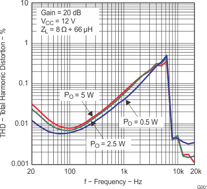
Figure 1. Total Harmonic Distortion vs Frequency (BTL)
TPA3110D2-Q1 g003_los528.gif
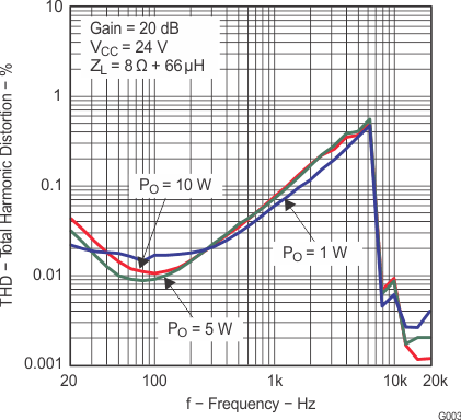
Figure 3. Total Harmonic Distortion vs Frequency (BTL)
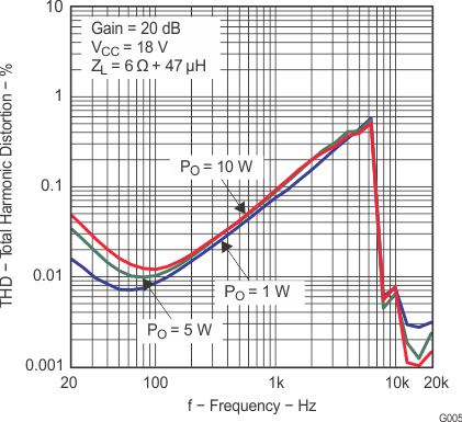
TPA3110D2-Q1 g005_los528.gif
Figure 5. Total Harmonic Distortion vs Frequency (BTL)
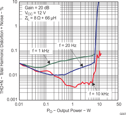
TPA3110D2-Q1 g007_los528.gif
Lighter color represents thermally limited region.
Figure 7. Total Harmonic Distortion + Noise vs Output Power (BTL)
TPA3110D2-Q1 g009_los528.gif
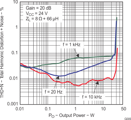
Figure 9. Total Harmonic Distortion + Noise vs Output Power (BTL)
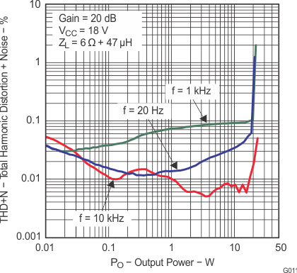
TPA3110D2-Q1 g011_los528.gif
Figure 11. Total Harmonic Distortion + Noise vs Output Power (BTL)
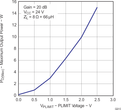
TPA3110D2-Q1 g013_los528.gif
Figure 13. Maximum Output Power vs PLIMIT Voltage (BTL)
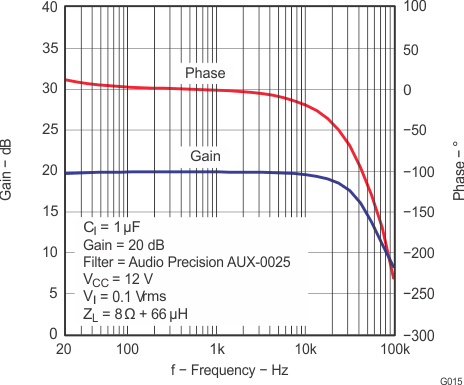
TPA3110D2-Q1 g015_los528.gif
Figure 15. Gain/Phase vs Frequency (BTL)
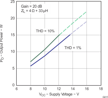
TPA3110D2-Q1 g017_los528.gif
Note: Dashed lines represent thermally limited regions.
Figure 17. Output Power vs Supply Voltage (BTL)
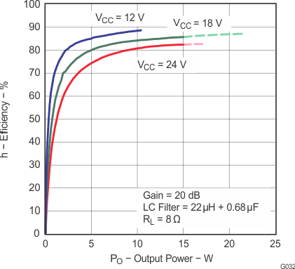
TPA3110D2-Q1 g032_los528.gif
Figure 19. Efficiency vs Output Power (BTL With LC Filter)
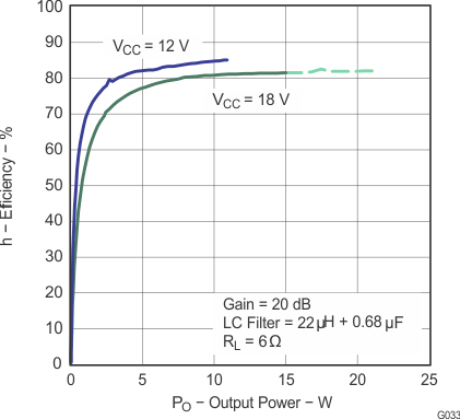
TPA3110D2-Q1 g033_los528.gif
Figure 21. Efficiency vs Output Power (BTL With LC Filter)
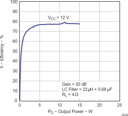
TPA3110D2-Q1 g034_los528.gif
Figure 23. Efficiency vs Output Power (BTL With LC Filter)
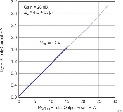
TPA3110D2-Q1 g022_los528.gif
Note: Dashed lines represent thermally limited regions.
Figure 25. Supply Current vs Total Output Power (BTL)
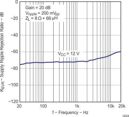
TPA3110D2-Q1 g024_los528.gif
Figure 27. Supply Ripple Rejection Ratio vs Frequency (BTL)
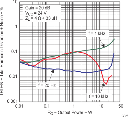
TPA3110D2-Q1 g026_los528.gif
Figure 29. Total Harmonic Distortion + Noise vs Output Power (PBTL)
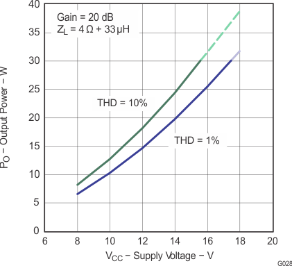
TPA3110D2-Q1 g028_los528.gif
Note: Dashed lines represent thermally limited regions.
Figure 31. Output Power vs Supply Voltage (PBTL)
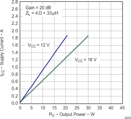
TPA3110D2-Q1 g030_los528.gif
Figure 33. Supply Current vs Output Power (PBTL)
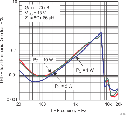
TPA3110D2-Q1 g002_los528.gif
Figure 2. Total Harmonic Distortion vs Frequency (BTL)
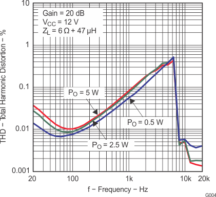
TPA3110D2-Q1 g004_los528.gif
Figure 4. Total Harmonic Distortion vs Frequency (BTL)
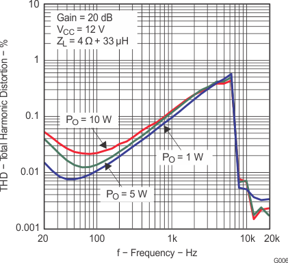
TPA3110D2-Q1 g006_los528.gif
Figure 6. Total Harmonic Distortion vs Frequency (BTL)
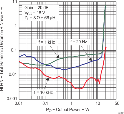
TPA3110D2-Q1 g008_los528.gif
Figure 8. Total Harmonic Distortion + Noise vs Output Power (BTL)
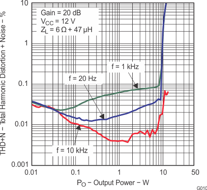
TPA3110D2-Q1 g010_los528.gif
Figure 10. Total Harmonic Distortion + Noise vs Output Power (BTL)
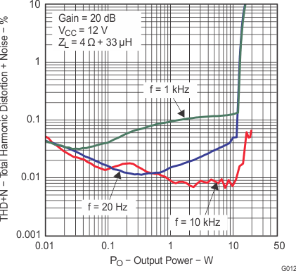
TPA3110D2-Q1 g012_los528.gif
Figure 12. Total Harmonic Distortion + Noise vs Output Power (BTL)
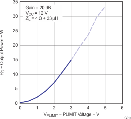
TPA3110D2-Q1 g014_los528.gif
Note: Dashed lines represent thermally limited regions.
Figure 14. Output Power vs PLIMIT Voltage (BTL)
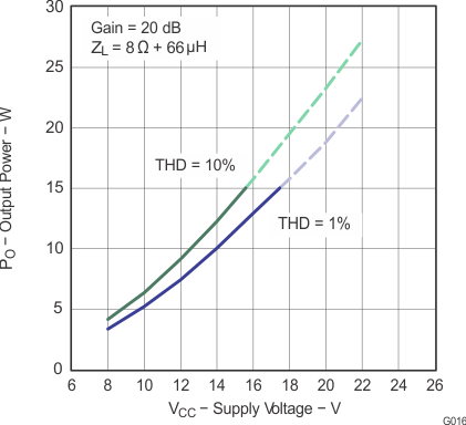
TPA3110D2-Q1 g016_los528.gif
Note: Dashed lines represent thermally limited regions.
Figure 16. Output Power vs Supply Voltage (BTL)
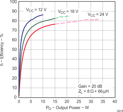
TPA3110D2-Q1 g018_los528.gif
Note: Dashed lines represent thermally limited regions.
Figure 18. Efficiency vs Output Power (BTL)
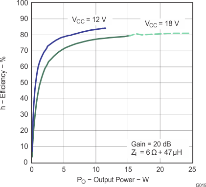
TPA3110D2-Q1 g019_los528.gif
Note: Dashed lines represent thermally limited regions.
Figure 20. Efficiency vs Output Power (BTL)
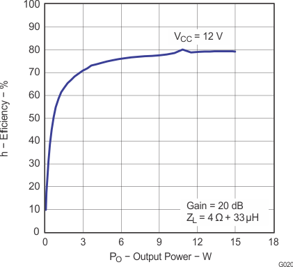
TPA3110D2-Q1 g020_los528.gif
Figure 22. Efficiency vs Output Power (BTL)
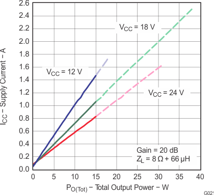
TPA3110D2-Q1 g021_los528.gif
Note: Dashed lines represent thermally limited regions.
Figure 24. Supply Current vs Total Output Power (BTL)
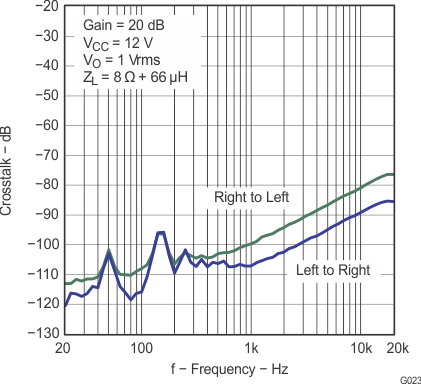
TPA3110D2-Q1 g023_los528.gif
Figure 26. Crosstalk vs Frequency (BTL)
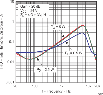
TPA3110D2-Q1 g025_los528.gif
Figure 28. Total Harmonic Distortion vs Frequency (PBTL)
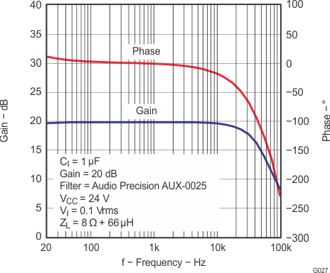
TPA3110D2-Q1 g027_los528.gif
Figure 30. Gain/Phase vs Frequency (PBTL)
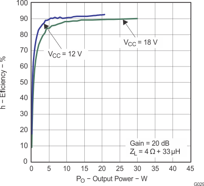
TPA3110D2-Q1 g029_los528.gif
Figure 32. Efficiency vs Output Power (PBTL)
TPA3110D2-Q1 g031_los528.gif
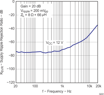
Figure 34. Supply Ripple Rejection Ratio vs Frequency (PBTL)