SLOS520A August 2007 – March 2016 TPA2013D1
PRODUCTION DATA.
- 1 Features
- 2 Applications
- 3 Description
- 4 Revision History
- 5 Device Comparison Table
- 6 Pin Configuration and Functions
-
7 Specifications
- 7.1 Absolute Maximum Ratings
- 7.2 ESD Ratings
- 7.3 Recommended Operating Conditions
- 7.4 Thermal Information
- 7.5 DC Characteristics
- 7.6 Boost Converter DC Characteristics
- 7.7 Class D Amplifier DC Characteristics
- 7.8 AC Characteristics
- 7.9 Class D Amplifier AC Characteristics
- 7.10 Dissipation Ratings
- 7.11 Typical Characteristics
- 8 Parameter Measurement Information
- 9 Detailed Description
-
10Application and Implementation
- 10.1 Application Information
- 10.2
Typical Applications
- 10.2.1
TPA2013D1 With Differential Input Signal
- 10.2.1.1 Design Requirements
- 10.2.1.2 Detailed Design Procedure
- 10.2.1.3 Application Curves
- 10.2.2 Bypassing the Boost Converter
- 10.2.3 Stereo Operation Application
- 10.2.4 LED Driver for Digital Still Cameras
- 10.2.5 Design Requirements
- 10.2.6 Detailed Design Procedure
- 10.2.7 Application Curves
- 10.2.1
TPA2013D1 With Differential Input Signal
- 11Power Supply Recommendations
- 12Layout
- 13Device and Documentation Support
- 14Mechanical, Packaging, and Orderable Information
封装选项
机械数据 (封装 | 引脚)
散热焊盘机械数据 (封装 | 引脚)
- RGP|20
订购信息
1 Features
- High Efficiency Integrated Boost Converter (Over 90% Efficiency)
- 2.2-W into an 8-Ω Load from a 3.6-V Supply
- 2.7-W into an 4-Ω Load from a 3.6-V Supply
- Operates from 1.8 V to 5.5 V
- Efficient Class-D Prolongs Battery Life
- Independent Shutdown for Boost Converter and Class-D Amplifier
- Differential Inputs Reduce RF Common Noise
- Built-In INPUT Low-Pass Filter Decreases RF and Out-of-Band Noise Sensitivity
- Synchronized Boost and Class-D Eliminates Beat Frequencies
- Thermal and Short-Circuit Protection
- Available in 2.275-mm × 2.275-mm 16-ball WCSP and 4-mm × 4-mm 20-Lead QFN Packages
- 3 Selectable Gain Settings of 2 V/V, 6 V/V, and
10 V/V
2 Applications
- Cell Phones
- PDA
- GPS
- Portable Electronics
3 Description
The TPA2013D1 device is a high efficiency Class-D audio power amplifier with an integrated boost converter. It drives up to 2.7 W (10% THD+N) into a 4-Ω speaker. With 85% typical efficiency, the TPA2013D1 helps extend battery life when playing audio.
The built-in boost converter generates the voltage rail for the Class-D amplifier. This provides a louder audio output than a stand-alone amplifier connected directly to the battery. It also maintains a consistent loudness, regardless of battery voltage. Additionally, the boost converter can be used to supply external devices.
The TPA2013D1 has an integrated low pass filter to improve RF rejection and reduce out-of-band noise, increasing the signal-to-noise ratio (SNR). A built-in PLL synchronizes the boost converter and Class-D switching frequencies, thus eliminating beat frequencies and improving audio quality. All outputs are fully protected against shorts to ground, power supply, and output-to-output shorts.
Device Information(1)
| PART NUMBER | PACKAGE | BODY SIZE (NOM) |
|---|---|---|
| TPA2013D1 | VQFN (20) | 4.00 mm × 4.00 mm |
| DSBGA (16) | 2.275 mm × 2.275 mm |
- For all available packages, see the orderable addendum at the end of the data sheet.
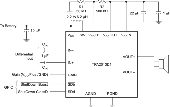
Simplified Application Schematic
