ZHCSLR4F december 2019 – july 2023 TMUX1308-Q1 , TMUX1309-Q1
PRODUCTION DATA
- 1
- 1 特性
- 2 应用
- 3 说明
- 4 Revision History
- 5 Device Comparison Table
- 6 Pin Configuration and Functions
-
7 Specifications
- 7.1 Absolute Maximum Ratings
- 7.2 ESD Ratings
- 7.3 Recommended Operating Conditions
- 7.4 Thermal Information: TMUX1308-Q1
- 7.5 Thermal Information: TMUX1309-Q1
- 7.6 Electrical Characteristics
- 7.7 Logic and Dynamic Characteristics
- 7.8 Timing Characteristics
- 7.9 Injection Current Coupling
- 7.10 Typical Characteristics
- 8 Parameter Measurement Information
-
9 Detailed Description
- 9.1 Overview
- 9.2 Functional Block Diagram
- 9.3
Feature Description
- 9.3.1 Bidirectional Operation
- 9.3.2 Rail-to-Rail Operation
- 9.3.3 1.8 V Logic Compatible Inputs
- 9.3.4 Fail-Safe Logic
- 9.3.5
Injection Current Control
- 9.3.5.1 TMUX13xx-Q1 is Powered, Channel is Unselected, and the Input Signal is Greater Than VDD (VDD = 5 V, VINPUT = 5.5 V)
- 9.3.5.2 TMUX13xx-Q1 is Powered, Channel is Selected, and the Input Signal is Greater Than VDD (VDD = 5 V, VINPUT = 5.5 V)
- 9.3.5.3 TMUX13xx-Q1 is Unpowered and the Input Signal has a Voltage Present (VDD = 0 V, VINPUT = 3 V)
- 9.4 Device Functional Modes
- 9.5 Truth Tables
- 10Application and Implementation
- 11Device and Documentation Support
- 12Mechanical, Packaging, and Orderable Information
封装选项
机械数据 (封装 | 引脚)
散热焊盘机械数据 (封装 | 引脚)
- BQB|16
订购信息
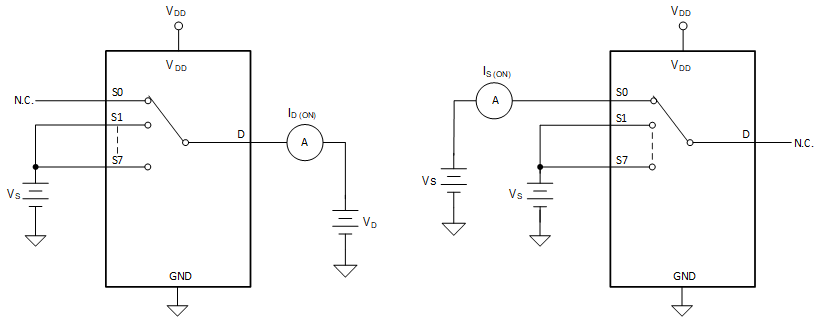
8.3 On-Leakage Current
Source on-leakage current is defined as the leakage current flowing into or out of the source pin when the switch is on. This current is denoted by the symbol IS(ON).
Drain on-leakage current is defined as the leakage current flowing into or out of the drain pin when the switch is on. This current is denoted by the symbol ID(ON).
Either the source pin or drain pin is left floating during the measurement. Figure 8-3 shows the circuit used for measuring the on-leakage current, denoted by IS(ON) or ID(ON).
 Figure 8-3 On-Leakage Measurement Setup