ZHCSK56A August 2019 – July 2020 TMUX1208-Q1
PRODUCTION DATA
- 1 特性
- 2 应用
- 3 说明
- 4 Revision History
- 5 Pin Configuration and Functions
-
6 Specifications
- 6.1 Absolute Maximum Ratings
- 6.2 ESD Ratings
- 6.3 Recommended Operating Conditions
- 6.4 Thermal Information
- 6.5 Electrical Characteristics (VDD = 5 V ±10 %)
- 6.6 Electrical Characteristics (VDD = 3.3 V ±10 %)
- 6.7 Electrical Characteristics (VDD = 1.8 V ±10 %)
- 6.8 Electrical Characteristics (VDD = 1.2 V ±10 %)
- 7 Parameter Measurement Information
- 8 Detailed Description
- 9 Power Supply Recommendations
- 10Layout
- 11Device and Documentation Support
- 12Electrostatic Discharge Caution
- 13Glossary
10.1.1 Layout Information
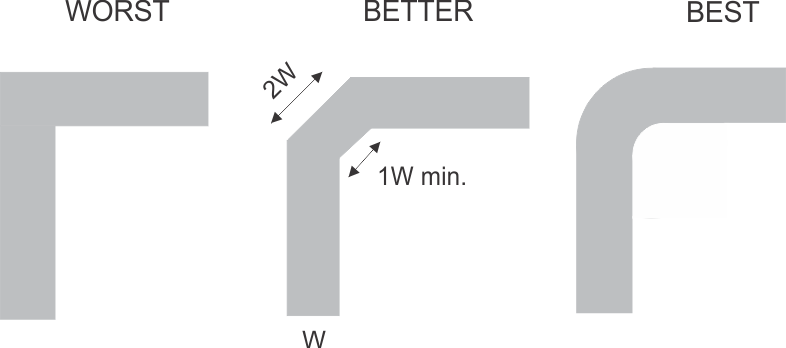
When a PCB trace turns a corner at a 90° angle, a reflection can occur. A reflection occurs primarily because of the change of width of the trace. At the apex of the turn, the trace width increases to 1.414 times the width. This increase upsets the transmission-line characteristics, especially the distributed capacitance and self–inductance of the trace which results in the reflection. Not all PCB traces can be straight and therefore some traces must turn corners. Figure 10-1 shows progressively better techniques of rounding corners. Only the last example (BEST) maintains constant trace width and minimizes reflections.
 Figure 10-1 Trace Example
Route high-speed signals using a minimum of vias and corners which reduces signal reflections and impedance changes. When a via must be used, increase the clearance size around it to minimize its capacitance. Each via introduces discontinuities in the signal’s transmission line and increases the chance of picking up interference from the other layers of the board. Be careful when designing test points, through-hole pins are not recommended at high frequencies.