ZHCS898O October 2003 – March 2019 TMS320F2801 , TMS320F28015 , TMS320F28016 , TMS320F2802 , TMS320F2806 , TMS320F2808 , TMS320F2809
PRODUCTION DATA.
- 1器件概述
- 2修订历史记录
- 3Device Comparison
- 4Terminal Configuration and Functions
-
5Specifications
- 5.1 Absolute Maximum Ratings
- 5.2 ESD Ratings – Automotive
- 5.3 ESD Ratings – Commercial
- 5.4 Recommended Operating Conditions
- 5.5
Power Consumption Summary
- Table 5-1 TMS320F2809, TMS320F2808 Current Consumption by Power-Supply Pins at 100-MHz SYSCLKOUT
- Table 5-2 TMS320F2806 Current Consumption by Power-Supply Pins at 100-MHz SYSCLKOUT
- Table 5-3 TMS320F2802, TMS320F2801 Current Consumption by Power-Supply Pins at 100-MHz SYSCLKOUT
- Table 5-4 TMS320C2802, TMS320C2801 Current Consumption by Power-Supply Pins at 100-MHz SYSCLKOUT
- 5.5.1 Reducing Current Consumption
- 5.5.2 Current Consumption Graphs
- 5.6 Electrical Characteristics
- 5.7 Thermal Resistance Characteristics for F280x 100-Ball GGM Package
- 5.8 Thermal Resistance Characteristics for F280x 100-Pin PZ Package
- 5.9 Thermal Resistance Characteristics for C280x 100-Ball GGM Package
- 5.10 Thermal Resistance Characteristics for C280x 100-Pin PZ Package
- 5.11 Thermal Resistance Characteristics for F2809 100-Ball GGM Package
- 5.12 Thermal Resistance Characteristics for F2809 100-Pin PZ Package
- 5.13 Thermal Design Considerations
- 5.14
Timing and Switching Characteristics
- 5.14.1 Timing Parameter Symbology
- 5.14.2 Power Sequencing
- 5.14.3 Clock Requirements and Characteristics
- 5.14.4
Peripherals
- 5.14.4.1 General-Purpose Input/Output (GPIO)
- 5.14.4.2 Enhanced Control Peripherals
- 5.14.4.3 External Interrupt Timing
- 5.14.4.4 I2C Electrical Specification and Timing
- 5.14.4.5 Serial Peripheral Interface (SPI) Timing
- 5.14.5 Emulator Connection Without Signal Buffering for the DSP
- 5.14.6 Flash Timing
- 5.15 On-Chip Analog-to-Digital Converter
- 5.16 Migrating From F280x Devices to C280x Devices
- 5.17 ROM Timing (C280x only)
-
6Detailed Description
- 6.1
Brief Descriptions
- 6.1.1 C28x CPU
- 6.1.2 Memory Bus (Harvard Bus Architecture)
- 6.1.3 Peripheral Bus
- 6.1.4 Real-Time JTAG and Analysis
- 6.1.5 Flash
- 6.1.6 ROM
- 6.1.7 M0, M1 SARAMs
- 6.1.8 L0, L1, H0 SARAMs
- 6.1.9 Boot ROM
- 6.1.10 Security
- 6.1.11 Peripheral Interrupt Expansion (PIE) Block
- 6.1.12 External Interrupts (XINT1, XINT2, XNMI)
- 6.1.13 Oscillator and PLL
- 6.1.14 Watchdog
- 6.1.15 Peripheral Clocking
- 6.1.16 Low-Power Modes
- 6.1.17 Peripheral Frames 0, 1, 2 (PFn)
- 6.1.18 General-Purpose Input/Output (GPIO) Multiplexer
- 6.1.19 32-Bit CPU-Timers (0, 1, 2)
- 6.1.20 Control Peripherals
- 6.1.21 Serial Port Peripherals
- 6.2
Peripherals
- 6.2.1 32-Bit CPU-Timers 0/1/2
- 6.2.2 Enhanced PWM Modules (ePWM1/2/3/4/5/6)
- 6.2.3 Hi-Resolution PWM (HRPWM)
- 6.2.4 Enhanced CAP Modules (eCAP1/2/3/4)
- 6.2.5 Enhanced QEP Modules (eQEP1/2)
- 6.2.6 Enhanced Analog-to-Digital Converter (ADC) Module
- 6.2.7 Enhanced Controller Area Network (eCAN) Modules (eCAN-A and eCAN-B)
- 6.2.8 Serial Communications Interface (SCI) Modules (SCI-A, SCI-B)
- 6.2.9 Serial Peripheral Interface (SPI) Modules (SPI-A, SPI-B, SPI-C, SPI-D)
- 6.2.10 Inter-Integrated Circuit (I2C)
- 6.2.11 GPIO MUX
- 6.3 Memory Maps
- 6.4 Register Map
- 6.5 Interrupts
- 6.6 System Control
- 6.7 Low-Power Modes Block
- 6.1
Brief Descriptions
- 7Applications, Implementation, and Layout
- 8器件和文档支持
- 9机械、封装和可订购信息
封装选项
请参考 PDF 数据表获取器件具体的封装图。
机械数据 (封装 | 引脚)
- PZ|100
- NMF|100
散热焊盘机械数据 (封装 | 引脚)
订购信息
6.3 Memory Maps
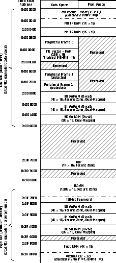
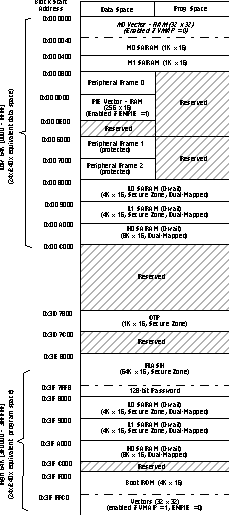
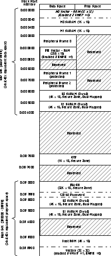
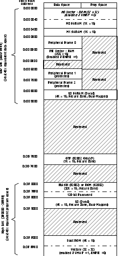
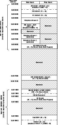
Table 6-18 Addresses of Flash Sectors in F2809
| ADDRESS RANGE | PROGRAM AND DATA SPACE |
|---|---|
| 0x3D 8000 – 0x3D BFFF | Sector H (16K x 16) |
| 0x3D C000 – 0x3D FFFF | Sector G (16K x 16) |
| 0x3E 0000 – 0x3E 3FFF | Sector F (16K x 16) |
| 0x3E 4000 – 0x3E 7FFF | Sector E (16K x 16) |
| 0x3E 8000 – 0x3E BFFF | Sector D (16K x 16) |
| 0x3E C000 – 0x3E FFFF | Sector C (16K x 16) |
| 0x3F 0000 – 0x3F 3FFF | Sector B (16K x 16) |
| 0x3F 4000 – 0x3F 7F7F | Sector A (16K x 16) |
| 0x3F 7F80 – 0x3F 7FF5 | Program to 0x0000 when using the
Code Security Module |
| 0x3F 7FF6 – 0x3F 7FF7 | Boot-to-Flash Entry Point
(program branch instruction here) |
| 0x3F 7FF8 – 0x3F 7FFF | Security Password (128-Bit)
(Do not program to all zeros) |
Table 6-19 Addresses of Flash Sectors in F2808
| ADDRESS RANGE | PROGRAM AND DATA SPACE |
|---|---|
| 0x3E 8000 – 0x3E BFFF | Sector D (16K x 16) |
| 0x3E C000 – 0x3E FFFF | Sector C (16K x 16) |
| 0x3F 0000 – 0x3F 3FFF | Sector B (16K x 16) |
| 0x3F 4000 – 0x3F 7F7F | Sector A (16K x 16) |
| 0x3F 7F80 – 0x3F 7FF5 | Program to 0x0000 when using the
Code Security Module |
| 0x3F 7FF6 – 0x3F 7FF7 | Boot-to-Flash Entry Point
(program branch instruction here) |
| 0x3F 7FF8 – 0x3F 7FFF | Security Password (128-Bit)
(Do not program to all zeros) |
Table 6-20 Addresses of Flash Sectors in F2806, F2802
| ADDRESS RANGE | PROGRAM AND DATA SPACE |
|---|---|
| 0x3F 0000 – 0x3F 1FFF | Sector D (8K x 16) |
| 0x3F 2000 – 0x3F 3FFF | Sector C (8K x 16) |
| 0x3F 4000 – 0x3F 5FFF | Sector B (8K x 16) |
| 0x3F 6000 – 0x3F 7F7F | Sector A (8K x 16) |
| 0x3F 7F80 – 0x3F 7FF5 | Program to 0x0000 when using the
Code Security Module |
| 0x3F 7FF6 – 0x3F 7FF7 | Boot-to-Flash Entry Point
(program branch instruction here) |
| 0x3F 7FF8 – 0x3F 7FFF | Security Password (128-Bit)
(Do not program to all zeros) |
Table 6-21 Addresses of Flash Sectors in F2801, F28015, F28016
| ADDRESS RANGE | PROGRAM AND DATA SPACE |
|---|---|
| 0x3F 4000 – 0x3F 4FFF | Sector D (4K x 16) |
| 0x3F 5000 – 0x3F 5FFF | Sector C (4K x 16) |
| 0x3F 6000 – 0x3F 6FFF | Sector B (4K x 16) |
| 0x3F 7000 – 0x3F 7F7F | Sector A (4K x 16) |
| 0x3F 7F80 – 0x3F 7FF5 | Program to 0x0000 when using the
Code Security Module |
| 0x3F 7FF6 – 0x3F 7FF7 | Boot-to-Flash Entry Point
(program branch instruction here) |
| 0x3F 7FF8 – 0x3F 7FFF | Security Password (128-Bit)
(Do not program to all zeros) |
NOTE
- When the code-security passwords are programmed, all addresses between 0x3F7F80 and 0x3F7FF5 cannot be used as program code or data. These locations must be programmed to 0x0000.
- If the code security feature is not used, addresses 0x3F7F80 through 0x3F7FEF may be used for code or data. Addresses 0x3F7FF0 – 0x3F7FF5 are reserved for data and should not contain program code.
- On ROM devices, addresses 0x3F7FF0 – 0x3F7FF5 and 0x3D7BFC – 0x3D7BFF are reserved for TI, irrespective of whether code security has been used or not. User application should not use these locations in any way.
Table 6-22 shows how to handle these memory locations.
Table 6-22 Impact of Using the Code Security Module
| ADDRESS | FLASH | ROM | ||
|---|---|---|---|---|
| Code security enabled | Code security disabled | Code security enabled | Code security disabled | |
| 0x3F 7F80 – 0x3F 7FEF | Fill with 0x0000 | Application code and data | Fill with 0x0000 | Application code and data |
| 0x3F 7FF0 – 0x3F 7FF5 | Reserved for data only | Reserved for TI. Do not use. | ||
| 0x3D 7BFC – 0x3D 7BFF | Application code and data | |||
Peripheral Frame 1 and Peripheral Frame 2 are grouped together so as to enable these blocks to be write/read peripheral block protected. The protected mode ensures that all accesses to these blocks happen as written. Because of the C28x pipeline, a write immediately followed by a read, to different memory locations, will appear in reverse order on the memory bus of the CPU. This can cause problems in certain peripheral applications where the user expected the write to occur first (as written). The C28x CPU supports a block protection mode where a region of memory can be protected so as to make sure that operations occur as written (the penalty is extra cycles are added to align the operations). This mode is programmable and by default, it will protect the selected zones.
The wait-states for the various spaces in the memory map area are listed in Table 6-23.
Table 6-23 Wait-states
| AREA | WAIT-STATES | COMMENTS |
|---|---|---|
| M0 and M1 SARAMs | 0-wait | Fixed |
| Peripheral Frame 0 | 0-wait | Fixed |
| Peripheral Frame 1 | 0-wait (writes)
2-wait (reads) |
Fixed. The eCAN peripheral can extend a cycle as needed. Back-to-back writes will introduce a 1-cycle delay. |
| Peripheral Frame 2 | 0-wait (writes)
2-wait (reads) |
Fixed |
| L0 and L1 SARAMs | 0-wait | |
| OTP | Programmable,
1-wait minimum |
Programmed via the Flash registers. 1-wait-state operation is possible at a reduced CPU frequency. See Section 6.1.5 for more information. |
| Flash | Programmable,
0-wait minimum |
Programmed via the Flash registers. 0-wait-state operation is possible at reduced CPU frequency. The CSM password locations are hardwired for 16 wait-states. See Section 6.1.5 for more information. |
| H0 SARAM | 0-wait | Fixed |
| Boot-ROM | 1-wait | Fixed |