ZHCS009J November   2010  – September 2021 TMS320F28062 , TMS320F28062F , TMS320F28063 , TMS320F28064 , TMS320F28065 , TMS320F28066 , TMS320F28067 , TMS320F28068F , TMS320F28068M , TMS320F28069 , TMS320F28069F , TMS320F28069M

PRODUCTION DATA  

  1. 特性
  2. 应用
  3. 说明
    1. 3.1 功能方框图
    2. 3.2 系统器件图
  4. Revision History
  5. Device Comparison
    1. 5.1 Related Products
  6. Terminal Configuration and Functions
    1. 6.1 Pin Diagrams
    2. 6.2 Signal Descriptions
      1. 6.2.1 Signal Descriptions
  7. Specifications
    1. 7.1  Absolute Maximum Ratings
    2. 7.2  ESD Ratings – Commercial
    3. 7.3  ESD Ratings – Automotive
    4. 7.4  Recommended Operating Conditions
    5. 7.5  Power Consumption Summary
      1. 7.5.1 TMS320F2806x Current Consumption at 90-MHz SYSCLKOUT
      2. 7.5.2 Reducing Current Consumption
      3. 7.5.3 Current Consumption Graphs (VREG Enabled)
    6. 7.6  Electrical Characteristics
    7. 7.7  Thermal Resistance Characteristics
      1. 7.7.1 PFP PowerPAD Package
      2. 7.7.2 PZP PowerPAD Package
      3. 7.7.3 PN Package
      4. 7.7.4 PZ Package
    8. 7.8  Thermal Design Considerations
    9. 7.9  Debug Probe Connection Without Signal Buffering for the MCU
    10. 7.10 Parameter Information
      1. 7.10.1 Timing Parameter Symbology
      2. 7.10.2 General Notes on Timing Parameters
    11. 7.11 Test Load Circuit
    12. 7.12 Power Sequencing
      1. 7.12.1 Reset ( XRS) Timing Requirements
      2. 7.12.2 Reset ( XRS) Switching Characteristics
    13. 7.13 Clock Specifications
      1. 7.13.1 Device Clock Table
        1. 7.13.1.1 2806x Clock Table and Nomenclature (90-MHz Devices)
        2. 7.13.1.2 Device Clocking Requirements/Characteristics
        3. 7.13.1.3 Internal Zero-Pin Oscillator (INTOSC1/INTOSC2) Characteristics
      2. 7.13.2 Clock Requirements and Characteristics
        1. 7.13.2.1 XCLKIN Timing Requirements – PLL Enabled
        2. 7.13.2.2 XCLKIN Timing Requirements – PLL Disabled
        3. 7.13.2.3 XCLKOUT Switching Characteristics (PLL Bypassed or Enabled)
    14. 7.14 Flash Timing
      1. 7.14.1 Flash/OTP Endurance for T Temperature Material
      2. 7.14.2 Flash/OTP Endurance for S Temperature Material
      3. 7.14.3 Flash/OTP Endurance for Q Temperature Material
      4. 7.14.4 Flash Parameters at 90-MHz SYSCLKOUT
      5. 7.14.5 Flash/OTP Access Timing
      6. 7.14.6 Flash Data Retention Duration
  8. Detailed Description
    1. 8.1 Overview
      1. 8.1.1  CPU
      2. 8.1.2  Control Law Accelerator (CLA)
      3. 8.1.3  Viterbi, Complex Math, CRC Unit (VCU)
      4. 8.1.4  Memory Bus (Harvard Bus Architecture)
      5. 8.1.5  Peripheral Bus
      6. 8.1.6  Real-Time JTAG and Analysis
      7. 8.1.7  Flash
      8. 8.1.8  M0, M1 SARAMs
      9. 8.1.9  L4 SARAM, and L0, L1, L2, L3, L5, L6, L7, and L8 DPSARAMs
      10. 8.1.10 Boot ROM
        1. 8.1.10.1 Debug Boot
        2. 8.1.10.2 GetMode
        3. 8.1.10.3 Peripheral Pins Used by the Bootloader
      11. 8.1.11 Security
      12. 8.1.12 Peripheral Interrupt Expansion (PIE) Block
      13. 8.1.13 External Interrupts (XINT1 to XINT3)
      14. 8.1.14 Internal Zero Pin Oscillators, Oscillator, and PLL
      15. 8.1.15 Watchdog
      16. 8.1.16 Peripheral Clocking
      17. 8.1.17 Low-power Modes
      18. 8.1.18 Peripheral Frames 0, 1, 2, 3 (PFn)
      19. 8.1.19 General-Purpose Input/Output (GPIO) Multiplexer
      20. 8.1.20 32-Bit CPU-Timers (0, 1, 2)
      21. 8.1.21 Control Peripherals
      22. 8.1.22 Serial Port Peripherals
    2. 8.2 Memory Maps
    3. 8.3 Register Maps
    4. 8.4 Device Debug Registers
    5. 8.5 VREG, BOR, POR
      1. 8.5.1 On-chip VREG
        1. 8.5.1.1 Using the On-chip VREG
        2. 8.5.1.2 Disabling the On-chip VREG
      2. 8.5.2 On-chip Power-On Reset (POR) and Brownout Reset (BOR) Circuit
    6. 8.6 System Control
      1. 8.6.1 Internal Zero Pin Oscillators
      2. 8.6.2 Crystal Oscillator Option
      3. 8.6.3 PLL-Based Clock Module
      4. 8.6.4 USB and HRCAP PLL Module (PLL2)
      5. 8.6.5 Loss of Input Clock (NMI Watchdog Function)
      6. 8.6.6 CPU Watchdog Module
    7. 8.7 Low-power Modes Block
    8. 8.8 Interrupts
      1. 8.8.1 External Interrupts
        1. 8.8.1.1 External Interrupt Electrical Data/Timing
          1. 8.8.1.1.1 External Interrupt Timing Requirements
          2. 8.8.1.1.2 External Interrupt Switching Characteristics
    9. 8.9 Peripherals
      1. 8.9.1  CLA Overview
      2. 8.9.2  Analog Block
        1. 8.9.2.1 Analog-to-Digital Converter (ADC)
          1. 8.9.2.1.1 Features
          2. 8.9.2.1.2 ADC Start-of-Conversion Electrical Data/Timing
            1. 8.9.2.1.2.1 External ADC Start-of-Conversion Switching Characteristics
          3. 8.9.2.1.3 On-Chip Analog-to-Digital Converter (ADC) Electrical Data/Timing
            1. 8.9.2.1.3.1 ADC Electrical Characteristics
            2. 8.9.2.1.3.2 ADC Power Modes
            3. 8.9.2.1.3.3 Internal Temperature Sensor
              1. 8.9.2.1.3.3.1 Temperature Sensor Coefficient
            4. 8.9.2.1.3.4 ADC Power-Up Control Bit Timing
              1. 8.9.2.1.3.4.1 ADC Power-Up Delays
            5. 8.9.2.1.3.5 ADC Sequential and Simultaneous Timings
        2. 8.9.2.2 ADC MUX
        3. 8.9.2.3 Comparator Block
          1. 8.9.2.3.1 On-Chip Comparator/DAC Electrical Data/Timing
            1. 8.9.2.3.1.1 Electrical Characteristics of the Comparator/DAC
      3. 8.9.3  Detailed Descriptions
      4. 8.9.4  Serial Peripheral Interface (SPI) Module
        1. 8.9.4.1 SPI Master Mode Electrical Data/Timing
          1. 8.9.4.1.1 SPI Master Mode External Timing (Clock Phase = 0)
          2. 8.9.4.1.2 SPI Master Mode External Timing (Clock Phase = 1)
        2. 8.9.4.2 SPI Slave Mode Electrical Data/Timing
          1. 8.9.4.2.1 SPI Slave Mode External Timing (Clock Phase = 0)
          2. 8.9.4.2.2 SPI Slave Mode External Timing (Clock Phase = 1)
      5. 8.9.5  Serial Communications Interface (SCI) Module
      6. 8.9.6  Multichannel Buffered Serial Port (McBSP) Module
        1. 8.9.6.1 McBSP Electrical Data/Timing
          1. 8.9.6.1.1 McBSP Transmit and Receive Timing
            1. 8.9.6.1.1.1 McBSP Timing Requirements
            2. 8.9.6.1.1.2 McBSP Switching Characteristics
          2. 8.9.6.1.2 McBSP as SPI Master or Slave Timing
            1. 8.9.6.1.2.1 McBSP as SPI Master or Slave Timing Requirements (CLKSTP = 10b, CLKXP = 0)
            2. 8.9.6.1.2.2 McBSP as SPI Master or Slave Switching Characteristics (CLKSTP = 10b, CLKXP = 0)
            3. 8.9.6.1.2.3 McBSP as SPI Master or Slave Timing Requirements (CLKSTP = 11b, CLKXP = 0)
            4. 8.9.6.1.2.4 McBSP as SPI Master or Slave Switching Characteristics (CLKSTP = 11b, CLKXP = 0)
            5. 8.9.6.1.2.5 McBSP as SPI Master or Slave Timing Requirements (CLKSTP = 10b, CLKXP = 1)
            6. 8.9.6.1.2.6 McBSP as SPI Master or Slave Switching Characteristics (CLKSTP = 10b, CLKXP = 1)
            7. 8.9.6.1.2.7 McBSP as SPI Master or Slave Timing Requirements (CLKSTP = 11b, CLKXP = 1)
            8. 8.9.6.1.2.8 McBSP as SPI Master or Slave Switching Characteristics (CLKSTP = 11b, CLKXP = 1)
      7. 8.9.7  Enhanced Controller Area Network (eCAN) Module
      8. 8.9.8  Inter-Integrated Circuit (I2C)
        1. 8.9.8.1 I2C Electrical Data/Timing
          1. 8.9.8.1.1 I2C Timing Requirements
          2. 8.9.8.1.2 I2C Switching Characteristics
      9. 8.9.9  Enhanced Pulse Width Modulator (ePWM) Modules (ePWM1 to ePWM8)
        1. 8.9.9.1 ePWM Electrical Data/Timing
          1. 8.9.9.1.1 ePWM Timing Requirements
          2. 8.9.9.1.2 ePWM Switching Characteristics
        2. 8.9.9.2 Trip-Zone Input Timing
          1. 8.9.9.2.1 Trip-Zone Input Timing Requirements
      10. 8.9.10 High-Resolution PWM (HRPWM)
        1. 8.9.10.1 HRPWM Electrical Data/Timing
          1. 8.9.10.1.1 High-Resolution PWM Characteristics
      11. 8.9.11 Enhanced Capture Module (eCAP1)
        1. 8.9.11.1 eCAP Electrical Data/Timing
          1. 8.9.11.1.1 Enhanced Capture (eCAP) Timing Requirement
          2. 8.9.11.1.2 eCAP Switching Characteristics
      12. 8.9.12 High-Resolution Capture Modules (HRCAP1 to HRCAP4)
        1. 8.9.12.1 HRCAP Electrical Data/Timing
          1. 8.9.12.1.1 High-Resolution Capture (HRCAP) Timing Requirements
      13. 8.9.13 Enhanced Quadrature Encoder Modules (eQEP1, eQEP2)
        1. 8.9.13.1 eQEP Electrical Data/Timing
          1. 8.9.13.1.1 Enhanced Quadrature Encoder Pulse (eQEP) Timing Requirements
          2. 8.9.13.1.2 eQEP Switching Characteristics
      14. 8.9.14 JTAG Port
      15. 8.9.15 General-Purpose Input/Output (GPIO) MUX
        1. 8.9.15.1 GPIO Electrical Data/Timing
          1. 8.9.15.1.1 GPIO Output Timing
            1. 8.9.15.1.1.1 General-Purpose Output Switching Characteristics
          2. 8.9.15.1.2 GPIO Input Timing
            1. 8.9.15.1.2.1 General-Purpose Input Timing Requirements
          3. 8.9.15.1.3 Sampling Window Width for Input Signals
          4. 8.9.15.1.4 Low-Power Mode Wakeup Timing
            1. 8.9.15.1.4.1 IDLE Mode Timing Requirements
            2. 8.9.15.1.4.2 IDLE Mode Switching Characteristics
            3. 8.9.15.1.4.3 STANDBY Mode Timing Requirements
            4. 8.9.15.1.4.4 STANDBY Mode Switching Characteristics
            5. 8.9.15.1.4.5 HALT Mode Timing Requirements
            6. 8.9.15.1.4.6 HALT Mode Switching Characteristics
      16. 8.9.16 Universal Serial Bus (USB)
        1. 8.9.16.1 USB Electrical Data/Timing
          1. 8.9.16.1.1 USB Input Ports DP and DM Timing Requirements
          2. 8.9.16.1.2 USB Output Ports DP and DM Switching Characteristics
  9. Applications, Implementation, and Layout
    1. 9.1 TI Reference Design
  10. 10Device and Documentation Support
    1. 10.1 Device and Development Support Tool Nomenclature
    2. 10.2 Tools and Software
    3. 10.3 Documentation Support
    4. 10.4 支持资源
    5. 10.5 Trademarks
    6. 10.6 Electrostatic Discharge Caution
    7. 10.7 术语表
  11. 11Mechanical, Packaging, and Orderable Information
    1. 11.1 Packaging Information

封装选项

机械数据 (封装 | 引脚)
散热焊盘机械数据 (封装 | 引脚)
订购信息

Pin Diagrams

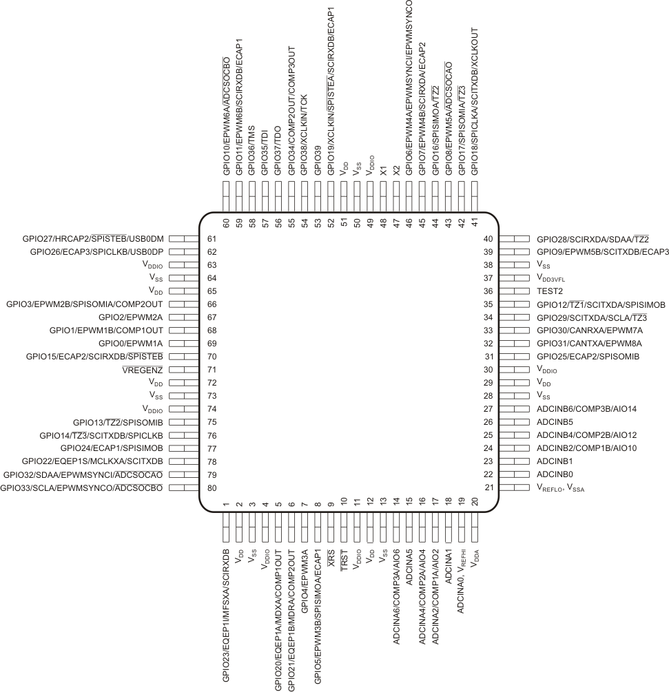
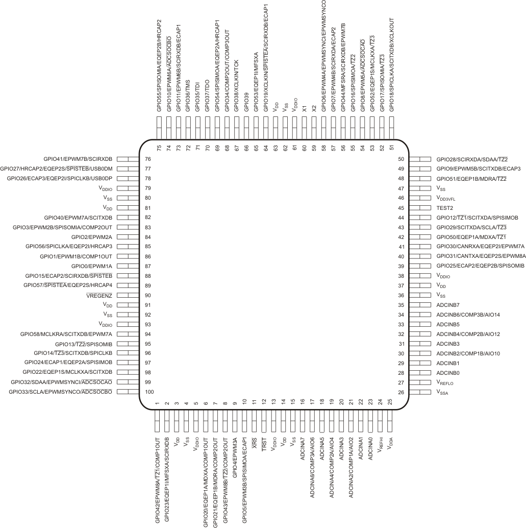
Figure 6-1 shows the pin assignments on the 80-pin PN and PFP packages. Figure 6-2 shows the pin assignments on the 100-pin PZ and PZP packages.
GUID-5A6079D7-9643-4E79-9815-C0D442125487-low.gif
Pin 19: VREFHI and ADCINA0 share the same pin on the 80-pin PN and PFP devices and their use is mutually exclusive to one another. Pin 21: VREFLO is always connected to VSSA on the 80-pin PN and PFP devices.
The PowerPAD is not connected to the ground on the die. To facilitate effective heat dissipation, the PowerPAD must be connected to the ground plane of the PCB. It should not be left unconnected. For more details, see PowerPAD™ Thermally Enhanced Package.
Figure 6-1 80-Pin PN and PFP Packages (Top View)
GUID-E60ECA64-BCB3-4C29-8876-D8263A6470DD-low.gif
The PowerPAD is not connected to the ground on the die. To facilitate effective heat dissipation, the PowerPAD must be connected to the ground plane of the PCB. It should not be left unconnected. For more details, see PowerPAD™ Thermally Enhanced Package.
Figure 6-2 100-Pin PZ and PZP Packages (Top View)
Note:

The PowerPAD™ should be soldered to the ground (GND) plane of the PCB because this will provide the best thermal conduction path. For this device, the PowerPAD is not electrically shorted to the internal die VSS; therefore, the PowerPAD does not provide an electrical connection to the PCB ground. To make optimum use of the thermal efficiencies designed into the PowerPAD package, the PCB must be designed with this technology in mind. A thermal land is required on the surface of the PCB directly underneath the body of the PowerPAD. The thermal land should be soldered to the exposed lead frame die pad of the PowerPad package; the thermal land should be as large as needed to dissipate the required heat. An array of thermal vias should be used to connect the thermal pad to the internal GND plane of the board. See PowerPAD™ Thermally Enhanced Package for more details on using the PowerPAD package.