ZHCSAH6F November   2012  – September 2021 TMS320F28050 , TMS320F28051 , TMS320F28052 , TMS320F28052F , TMS320F28052M , TMS320F28053 , TMS320F28054 , TMS320F28054F , TMS320F28054M , TMS320F28055

PRODUCTION DATA  

  1. 特性
  2. 应用
  3. 说明
    1. 3.1 功能方框图
  4. Revision History
  5. Device Comparison
    1. 5.1 Related Products
  6. Terminal Configuration and Functions
    1. 6.1 Pin Diagram
    2. 6.2 Signal Descriptions
      1. 6.2.1 Signal Descriptions
  7. Specifications
    1. 7.1  Absolute Maximum Ratings
    2. 7.2  ESD Ratings – Commercial
    3. 7.3  ESD Ratings – Automotive
    4. 7.4  Recommended Operating Conditions
    5. 7.5  Power Consumption Summary
      1. 7.5.1 TMS320F2805x Current Consumption at 60-MHz SYSCLKOUT
      2. 7.5.2 Reducing Current Consumption
      3. 7.5.3 Current Consumption Graphs (VREG Enabled)
    6. 7.6  Electrical Characteristics
    7. 7.7  Thermal Resistance Characteristics for PN Package
    8. 7.8  Thermal Design Considerations
    9. 7.9  JTAG Debug Probe Connection Without Signal Buffering for the MCU
    10. 7.10 Parameter Information
      1. 7.10.1 Timing Parameter Symbology
      2. 7.10.2 General Notes on Timing Parameters
    11. 7.11 Test Load Circuit
    12. 7.12 Power Sequencing
      1. 7.12.1 Reset ( XRS) Timing Requirements
      2. 7.12.2 Reset ( XRS) Switching Characteristics
    13. 7.13 Clock Specifications
      1. 7.13.1 Device Clock Table
        1. 7.13.1.1 2805x Clock Table and Nomenclature (60-MHz Devices)
        2. 7.13.1.2 Device Clocking Requirements/Characteristics
        3. 7.13.1.3 Internal Zero-Pin Oscillator (INTOSC1, INTOSC2) Characteristics
      2. 7.13.2 Clock Requirements and Characteristics
        1. 7.13.2.1 XCLKIN Timing Requirements - PLL Enabled
        2. 7.13.2.2 XCLKIN Timing Requirements - PLL Disabled
        3. 7.13.2.3 XCLKOUT Switching Characteristics (PLL Bypassed or Enabled)
    14. 7.14 Flash Timing
      1. 7.14.1 Flash/OTP Endurance for T Temperature Material
      2. 7.14.2 Flash/OTP Endurance for S Temperature Material
      3. 7.14.3 Flash/OTP Endurance for Q Temperature Material
      4. 7.14.4 Flash Parameters at 60-MHz SYSCLKOUT
      5. 7.14.5 Flash/OTP Access Timing
      6. 7.14.6 Flash Data Retention Duration
  8. Detailed Description
    1. 8.1 Overview
      1. 8.1.1  CPU
      2. 8.1.2  Control Law Accelerator
      3. 8.1.3  Memory Bus (Harvard Bus Architecture)
      4. 8.1.4  Peripheral Bus
      5. 8.1.5  Real-Time JTAG and Analysis
      6. 8.1.6  Flash
      7. 8.1.7  M0, M1 SARAMs
      8. 8.1.8  L0 SARAM, and L1, L2, and L3 DPSARAMs
      9. 8.1.9  Boot ROM
        1. 8.1.9.1 Emulation Boot
        2. 8.1.9.2 GetMode
        3. 8.1.9.3 Peripheral Pins Used by the Bootloader
      10. 8.1.10 Security
      11. 8.1.11 Peripheral Interrupt Expansion Block
      12. 8.1.12 External Interrupts (XINT1 to XINT3)
      13. 8.1.13 Internal Zero-Pin Oscillators, Oscillator, and PLL
      14. 8.1.14 Watchdog
      15. 8.1.15 Peripheral Clocking
      16. 8.1.16 Low-power Modes
      17. 8.1.17 Peripheral Frames 0, 1, 2, 3 (PFn)
      18. 8.1.18 General-Purpose Input/Output Multiplexer
      19. 8.1.19 32-Bit CPU-Timers (0, 1, 2)
      20. 8.1.20 Control Peripherals
      21. 8.1.21 Serial Port Peripherals
    2. 8.2 Memory Maps
    3. 8.3 Register Map
    4. 8.4 Device Emulation Registers
    5. 8.5 VREG, BOR, POR
      1. 8.5.1 On-chip VREG
        1. 8.5.1.1 Using the On-chip VREG
        2. 8.5.1.2 Disabling the On-chip VREG
      2. 8.5.2 On-chip Power-On Reset and Brownout Reset Circuit
    6. 8.6 System Control
      1. 8.6.1 Internal Zero-Pin Oscillators
      2. 8.6.2 Crystal Oscillator Option
      3. 8.6.3 PLL-Based Clock Module
      4. 8.6.4 Loss of Input Clock (NMI-watchdog Function)
      5. 8.6.5 CPU-watchdog Module
    7. 8.7 Low-power Modes Block
    8. 8.8 Interrupts
      1. 8.8.1 External Interrupts
        1. 8.8.1.1 External Interrupt Electrical Data/Timing
          1. 8.8.1.1.1 External Interrupt Timing Requirements
          2. 8.8.1.1.2 External Interrupt Switching Characteristics
    9. 8.9 Peripherals
      1. 8.9.1  Control Law Accelerator
        1. 8.9.1.1 CLA Device-Specific Information
        2. 8.9.1.2 CLA Register Descriptions
      2. 8.9.2  Analog Block
        1. 8.9.2.1 Analog-to-Digital Converter
          1. 8.9.2.1.1 ADC Device-Specific Information
          2. 8.9.2.1.2 ADC Electrical Data/Timing
            1. 8.9.2.1.2.1 ADC Electrical Characteristics
            2. 8.9.2.1.2.2 ADC Power Modes
            3. 8.9.2.1.2.3 External ADC Start-of-Conversion Electrical Data/Timing
              1. 8.9.2.1.2.3.1 External ADC Start-of-Conversion Switching Characteristics
            4. 8.9.2.1.2.4 Internal Temperature Sensor
              1. 8.9.2.1.2.4.1 Temperature Sensor Coefficient
            5. 8.9.2.1.2.5 ADC Power-Up Control Bit Timing
              1. 8.9.2.1.2.5.1 ADC Power-Up Delays
            6. 8.9.2.1.2.6 ADC Sequential and Simultaneous Timings
        2. 8.9.2.2 Analog Front End
          1. 8.9.2.2.1 AFE Device-Specific Information
          2. 8.9.2.2.2 AFE Register Descriptions
          3. 8.9.2.2.3 PGA Electrical Data/Timing
          4. 8.9.2.2.4 Comparator Block Electrical Data/Timing
            1. 8.9.2.2.4.1 Electrical Characteristics of the Comparator/DAC
          5. 8.9.2.2.5 VREFOUT Buffered DAC Electrical Data
            1. 8.9.2.2.5.1 Electrical Characteristics of VREFOUT Buffered DAC
      3. 8.9.3  Detailed Descriptions
      4. 8.9.4  Serial Peripheral Interface
        1. 8.9.4.1 SPI Device-Specific Information
        2. 8.9.4.2 SPI Register Descriptions
        3. 8.9.4.3 SPI Master Mode Electrical Data/Timing
          1. 8.9.4.3.1 SPI Master Mode External Timing (Clock Phase = 0)
          2. 8.9.4.3.2 SPI Master Mode External Timing (Clock Phase = 1)
        4. 8.9.4.4 SPI Slave Mode Electrical Data/Timing
          1. 8.9.4.4.1 SPI Slave Mode External Timing (Clock Phase = 0)
          2. 8.9.4.4.2 SPI Slave Mode External Timing (Clock Phase = 1)
      5. 8.9.5  Serial Communications Interface
        1. 8.9.5.1 SCI Device-Specific Information
        2. 8.9.5.2 SCI Register Descriptions
      6. 8.9.6  Enhanced Controller Area Network
        1. 8.9.6.1 eCAN Device-Specific Information
        2. 8.9.6.2 eCAN Register Descriptions
      7. 8.9.7  Inter-Integrated Circuit
        1. 8.9.7.1 I2C Device-Specific Information
        2. 8.9.7.2 I2C Register Descriptions
        3. 8.9.7.3 I2C Electrical Data/Timing
          1. 8.9.7.3.1 I2C Timing Requirements
          2. 8.9.7.3.2 I2C Switching Characteristics
      8. 8.9.8  Enhanced Pulse Width Modulator
        1. 8.9.8.1 ePWM Device-Specific Information
        2. 8.9.8.2 ePWM Register Descriptions
        3. 8.9.8.3 ePWM Electrical Data/Timing
          1. 8.9.8.3.1 ePWM Timing Requirements
          2. 8.9.8.3.2 ePWM Switching Characteristics
          3. 8.9.8.3.3 Trip-Zone Input Timing
            1. 8.9.8.3.3.1 Trip-Zone Input Timing Requirements
      9. 8.9.9  Enhanced Capture Module
        1. 8.9.9.1 eCAP Module Device-Specific Information
        2. 8.9.9.2 eCAP Module Register Descriptions
        3. 8.9.9.3 eCAP Module Electrical Data/Timing
          1. 8.9.9.3.1 eCAP Timing Requirement
          2. 8.9.9.3.2 eCAP Switching Characteristics
      10. 8.9.10 Enhanced Quadrature Encoder Pulse
        1. 8.9.10.1 eQEP Device-Specific Information
        2. 8.9.10.2 eQEP Register Descriptions
        3. 8.9.10.3 eQEP Electrical Data/Timing
          1. 8.9.10.3.1 eQEP Timing Requirements
          2. 8.9.10.3.2 eQEP Switching Characteristics
      11. 8.9.11 JTAG Port
        1. 8.9.11.1 JTAG Port Device-Specific Information
      12. 8.9.12 General-Purpose Input/Output
        1. 8.9.12.1 GPIO Device-Specific Information
        2. 8.9.12.2 GPIO Register Descriptions
        3. 8.9.12.3 GPIO Electrical Data/Timing
          1. 8.9.12.3.1 GPIO - Output Timing
            1. 8.9.12.3.1.1 General-Purpose Output Switching Characteristics
          2. 8.9.12.3.2 GPIO - Input Timing
            1. 8.9.12.3.2.1 General-Purpose Input Timing Requirements
          3. 8.9.12.3.3 Sampling Window Width for Input Signals
          4. 8.9.12.3.4 Low-Power Mode Wakeup Timing
            1. 8.9.12.3.4.1 IDLE Mode Timing Requirements
            2. 8.9.12.3.4.2 IDLE Mode Switching Characteristics
            3. 8.9.12.3.4.3 STANDBY Mode Timing Requirements
            4. 8.9.12.3.4.4 STANDBY Mode Switching Characteristics
            5. 8.9.12.3.4.5 HALT Mode Timing Requirements
            6. 8.9.12.3.4.6 HALT Mode Switching Characteristics
  9. Applications, Implementation, and Layout
    1. 9.1 TI Reference Design
  10. 10Device and Documentation Support
    1. 10.1 Getting Started
    2. 10.2 Device and Development Support Tool Nomenclature
    3. 10.3 Tools and Software
    4. 10.4 Documentation Support
    5. 10.5 支持资源
    6. 10.6 Trademarks
    7. 10.7 Electrostatic Discharge Caution
    8. 10.8 术语表
  11. 11Mechanical, Packaging, and Orderable Information
    1. 11.1 Packaging Information

封装选项

机械数据 (封装 | 引脚)
散热焊盘机械数据 (封装 | 引脚)
订购信息
SPI Slave Mode External Timing (Clock Phase = 0)
NO.PARAMETER(1)(2)(3)(4)(5)MINMAXUNIT
12tc(SPC)SCycle time, SPICLK4tc(SYSCLK)ns
13tw(SPC1)SPulse duration, SPICLK first pulse2tc(SYSCLK) – 1ns
14tw(SPC2)SPulse duration, SPICLK second pulse2tc(SYSCLK) – 1ns
15td(SOMI)SDelay time, SPICLK to SPISOMI valid21ns
16tv(SOMI)SValid time, SPISOMI data valid after SPICLK0ns
19tsu(SIMO)SSetup time, SPISIMO valid before SPICLK1.5tc(SYSCLK)ns
20th(SIMO)SHold time, SPISIMO data valid after SPICLK1.5tc(SYSCLK)ns
25tsu(STE)SSetup time, SPISTE active before SPICLK1.5tc(SYSCLK)ns
26th(STE)SHold time, SPISTE inactive after SPICLK1.5tc(SYSCLK)ns
The MASTER / SLAVE bit (SPICTL.2) is cleared and the CLOCK PHASE bit (SPICTL.3) is cleared.
tc(SPC) = SPI clock cycle time = LSPCLK/4 or LSPCLK/(SPIBRR + 1)
tc(LCO) = LSPCLK cycle time
Internal clock prescalers must be adjusted such that the SPI clock speed is limited to the following SPI clock rate:
Master mode transmit 25-MHz MAX, master mode receive 12.5-MHz MAX
Slave mode transmit 12.5-MHz MAX, slave mode receive 12.5-MHz MAX.
The active edge of the SPICLK signal referenced is controlled by the CLOCK POLARITY bit (SPICCR.6).
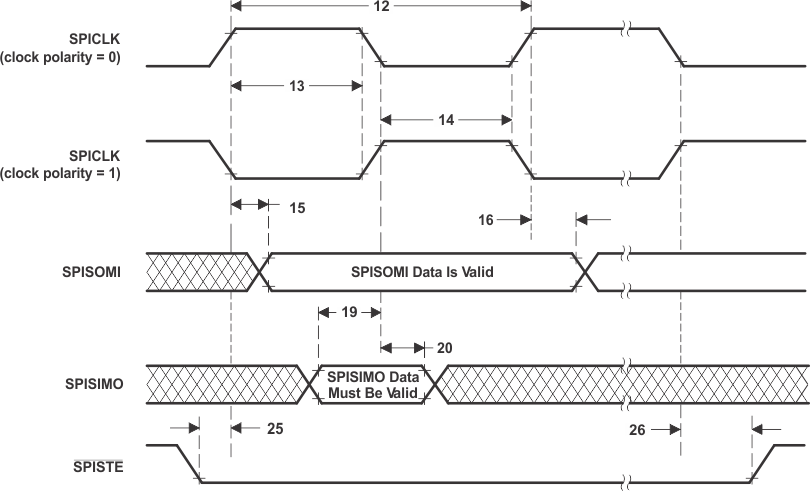
GUID-232D8749-6B3B-44AE-8CB5-279ABEC8B57F-low.gifFigure 8-31 SPI Slave Mode External Timing (Clock Phase = 0)