ZHCSA18F March 2009 – February 2021 TMS320C28341 , TMS320C28342 , TMS320C28343 , TMS320C28343-Q1 , TMS320C28344 , TMS320C28345 , TMS320C28346 , TMS320C28346-Q1
PRODUCTION DATA
- 1 特性
- 2 应用
- 3 说明
- 4 Revision History
- 5 Device Comparison
- 6 Terminal Configuration and Functions
-
7 Specifications
- 7.1 Absolute Maximum Ratings (1) (1)
- 7.2 ESD Ratings – Automotive
- 7.3 ESD Ratings – Commercial
- 7.4 Recommended Operating Conditions
- 7.5 Power Consumption Summary
- 7.6 Electrical Characteristics
- 7.7 Thermal Resistance Characteristics
- 7.8 Thermal Design Considerations
- 7.9
Timing and Switching Characteristics
- 7.9.1 Timing Parameter Symbology
- 7.9.2 Power Sequencing
- 7.9.3 Clock Requirements and Characteristics
- 7.9.4
Peripherals
- 7.9.4.1
General-Purpose Input/Output (GPIO)
- 7.9.4.1.1 GPIO - Output Timing
- 7.9.4.1.2 GPIO - Input Timing
- 7.9.4.1.3 Sampling Window Width for Input Signals
- 7.9.4.1.4
Low-Power Mode Wakeup Timing
- 7.9.4.1.4.1 IDLE Mode Timing Requirements (1)
- 7.9.4.1.4.2 IDLE Mode Switching Characteristics (1)
- 7.9.4.1.4.3 IDLE Mode Timing Diagram
- 7.9.4.1.4.4 STANDBY Mode Timing Requirements
- 7.9.4.1.4.5 STANDBY Mode Switching Characteristics
- 7.9.4.1.4.6 STANDBY Mode Timing Diagram
- 7.9.4.1.4.7 HALT Mode Timing Requirements
- 7.9.4.1.4.8 HALT Mode Switching Characteristics
- 7.9.4.1.4.9 HALT Mode Timing Diagram
- 7.9.4.2 Enhanced Control Peripherals
- 7.9.4.3 External Interrupt Timing
- 7.9.4.4 I2C Electrical Specification and Timing
- 7.9.4.5 Serial Peripheral Interface (SPI) Timing
- 7.9.4.6
Multichannel Buffered Serial Port (McBSP) Timing
- 7.9.4.6.1 McBSP Transmit and Receive Timing
- 7.9.4.6.2
McBSP as SPI Master or Slave Timing
- 7.9.4.6.2.1 McBSP as SPI Master or Slave Timing Requirements (CLKSTP = 10b, CLKXP = 0) (1)
- 7.9.4.6.2.2 McBSP as SPI Master or Slave Switching Characteristics (CLKSTP = 10b, CLKXP = 0)
- 7.9.4.6.2.3 McBSP as SPI Master or Slave Timing Requirements (CLKSTP = 11b, CLKXP = 0) (1)
- 7.9.4.6.2.4 McBSP as SPI Master or Slave Switching Characteristics (CLKSTP = 11b, CLKXP = 0)
- 7.9.4.6.2.5 McBSP as SPI Master or Slave Timing Requirements (CLKSTP = 10b, CLKXP = 1) (1)
- 7.9.4.6.2.6 McBSP as SPI Master or Slave Switching Characteristics (CLKSTP = 10b, CLKXP = 1)
- 7.9.4.6.2.7 McBSP as SPI Master or Slave Timing Requirements (CLKSTP = 11b, CLKXP = 1) (1)
- 7.9.4.6.2.8 McBSP as SPI Master or Slave Switching Characteristics (CLKSTP = 11b, CLKXP = 1) (1)
- 7.9.4.1
General-Purpose Input/Output (GPIO)
- 7.9.5 Emulator Connection Without Signal Buffering for the MCU
- 7.9.6
External Interface (XINTF) Timing
- 7.9.6.1 USEREADY = 0
- 7.9.6.2 Synchronous Mode (USEREADY = 1, READYMODE = 0)
- 7.9.6.3 Asynchronous Mode (USEREADY = 1, READYMODE = 1)
- 7.9.6.4 XINTF Signal Alignment to XCLKOUT
- 7.9.6.5 External Interface Read Timing
- 7.9.6.6 External Interface Write Timing
- 7.9.6.7
External Interface Ready-on-Read Timing With One External Wait State
- 7.9.6.7.1 External Interface Read Switching Characteristics (Ready-on-Read, One Wait State)
- 7.9.6.7.2 External Interface Read Timing Requirements (Ready-on-Read, One Wait State)
- 7.9.6.7.3 Synchronous XREADY Timing Requirements (Ready-on-Read, One Wait State) (1)
- 7.9.6.7.4 Asynchronous XREADY Timing Requirements (Ready-on-Read, One Wait State)
- 7.9.6.8 External Interface Ready-on-Write Timing With One External Wait State
- 7.9.6.9 XHOLD and XHOLDA Timing
-
8 Detailed Description
- 8.1
Brief Descriptions
- 8.1.1 C28x CPU
- 8.1.2 Memory Bus (Harvard Bus Architecture)
- 8.1.3 Peripheral Bus
- 8.1.4 Real-Time JTAG and Analysis
- 8.1.5 External Interface (XINTF)
- 8.1.6 M0, M1 SARAMs
- 8.1.7 L0, L1, L2, L3, L4, L5, L6, L7, H0, H1, H2, H3, H4, H5 SARAMs
- 8.1.8 Boot ROM
- 8.1.9 Security
- 8.1.10 Peripheral Interrupt Expansion (PIE) Block
- 8.1.11 External Interrupts (XINT1–XINT7, XNMI)
- 8.1.12 Oscillator and PLL
- 8.1.13 Watchdog
- 8.1.14 Peripheral Clocking
- 8.1.15 Low-Power Modes
- 8.1.16 Peripheral Frames 0, 1, 2, 3 (PFn)
- 8.1.17 General-Purpose Input/Output (GPIO) Multiplexer
- 8.1.18 32-Bit CPU-Timers (0, 1, 2)
- 8.1.19 Control Peripherals
- 8.1.20 Serial Port Peripherals
- 8.2
Peripherals
- 8.2.1 DMA Overview
- 8.2.2 32-Bit CPU-Timer 0, CPU-Timer 1, CPU-Timer 2
- 8.2.3 Enhanced PWM Modules
- 8.2.4 High-Resolution PWM (HRPWM)
- 8.2.5 Enhanced CAP Modules
- 8.2.6 Enhanced QEP Modules
- 8.2.7 External ADC Interface
- 8.2.8 Multichannel Buffered Serial Port (McBSP) Module
- 8.2.9 Enhanced Controller Area Network (eCAN) Modules (eCAN-A and eCAN-B)
- 8.2.10 Serial Communications Interface (SCI) Modules (SCI-A, SCI-B, SCI-C)
- 8.2.11 Serial Peripheral Interface (SPI) Module (SPI-A, SPI-D)
- 8.2.12 Inter-Integrated Circuit (I2C)
- 8.2.13 GPIO MUX
- 8.2.14 External Interface (XINTF)
- 8.3 Memory Maps
- 8.4 Register Map
- 8.5 Interrupts
- 8.6 System Control
- 8.7 Low-Power Modes Block
- 8.1
Brief Descriptions
- 9 Applications, Implementation, and Layout
- 10Device and Documentation Support
- 11Mechanical, Packaging, and Orderable Information
8.2.11 Serial Peripheral Interface (SPI) Module (SPI-A, SPI-D)
The device includes the four-pin serial peripheral interface (SPI) module. Two SPI modules (SPI-A and SPI-D) are available. The SPI is a high-speed, synchronous serial I/O port that allows a serial bit stream of programmed length (1 to 16 bits) to be shifted into and out of the device at a programmable bit-transfer rate. Normally, the SPI is used for communications between the MCU controller and external peripherals or another processor. Typical applications include external I/O or peripheral expansion through devices such as shift registers, display drivers, and ADCs. Multidevice communications are supported by the master/slave operation of the SPI.
The SPI module features include:
- Four external pins:
- SPISOMI: SPI slave-output/master-input pin
- SPISIMO: SPI slave-input/master-output pin
- SPISTE: SPI slave transmit-enable pin
- SPICLK: SPI serial-clock pin
All four pins can be used as GPIO if the SPI module is not used.
- Two operational modes: master and slave
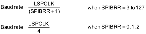
Baud rate: 125 different programmable rates.
 Note:
Note:See Section 7 for maximum I/O pin toggling speed.
- Data word length: 1 to 16 data bits
- Four clocking schemes (controlled by clock polarity and clock phase bits) include:
- Falling edge without phase delay: SPICLK active-high. SPI transmits data on the falling edge of the SPICLK signal and receives data on the rising edge of the SPICLK signal.
- Falling edge with phase delay: SPICLK active-high. SPI transmits data one half-cycle ahead of the falling edge of the SPICLK signal and receives data on the falling edge of the SPICLK signal.
- Rising edge without phase delay: SPICLK inactive-low. SPI transmits data on the rising edge of the SPICLK signal and receives data on the falling edge of the SPICLK signal.
- Rising edge with phase delay: SPICLK inactive-low. SPI transmits data one half-cycle ahead of the rising edge of the SPICLK signal and receives data on the rising edge of the SPICLK signal.
- Simultaneous receive and transmit operation (transmit function can be disabled in software)
- Transmitter and receiver operations are accomplished through either interrupt-driven or polled algorithms.
- Nine SPI module control registers: Located in control register frame beginning at address 7040h.
Note:
All registers in this module are 16-bit registers that are connected to Peripheral Frame 2. When a register is accessed, the register data is in the lower byte (7–0), and the upper byte (15–8) is read as zeros. Writing to the upper byte has no effect.
Enhanced features:
- 16-level transmit/receive FIFO
- Delayed transmit control
The SPI port operation is configured and controlled by the registers listed in Table 8-14 and Table 8-15.
| NAME | ADDRESS | SIZE (x16) | DESCRIPTION(1) |
|---|---|---|---|
| SPICCR | 0x7040 | 1 | SPI-A Configuration Control Register |
| SPICTL | 0x7041 | 1 | SPI-A Operation Control Register |
| SPISTS | 0x7042 | 1 | SPI-A Status Register |
| SPIBRR | 0x7044 | 1 | SPI-A Baud Rate Register |
| SPIRXEMU | 0x7046 | 1 | SPI-A Receive Emulation Buffer Register |
| SPIRXBUF | 0x7047 | 1 | SPI-A Serial Input Buffer Register |
| SPITXBUF | 0x7048 | 1 | SPI-A Serial Output Buffer Register |
| SPIDAT | 0x7049 | 1 | SPI-A Serial Data Register |
| SPIFFTX | 0x704A | 1 | SPI-A FIFO Transmit Register |
| SPIFFRX | 0x704B | 1 | SPI-A FIFO Receive Register |
| SPIFFCT | 0x704C | 1 | SPI-A FIFO Control Register |
| SPIPRI | 0x704F | 1 | SPI-A Priority Control Register |
| NAME | ADDRESS | SIZE (x16) | DESCRIPTION(1) |
|---|---|---|---|
| SPICCR | 0x7780 | 1 | SPI-D Configuration Control Register |
| SPICTL | 0x7781 | 1 | SPI-D Operation Control Register |
| SPISTS | 0x7782 | 1 | SPI-D Status Register |
| SPIBRR | 0x7784 | 1 | SPI-D Baud Rate Register |
| SPIRXEMU | 0x7786 | 1 | SPI-D Receive Emulation Buffer Register |
| SPIRXBUF | 0x7787 | 1 | SPI-D Serial Input Buffer Register |
| SPITXBUF | 0x7788 | 1 | SPI-D Serial Output Buffer Register |
| SPIDAT | 0x7789 | 1 | SPI-D Serial Data Register |
| SPIFFTX | 0x778A | 1 | SPI-D FIFO Transmit Register |
| SPIFFRX | 0x778B | 1 | SPI-D FIFO Receive Register |
| SPIFFCT | 0x778C | 1 | SPI-D FIFO Control Register |
| SPIPRI | 0x778F | 1 | SPI-D Priority Control Register |
Figure 8-14 is a block diagram of the SPI in slave mode.
")